Reset, Clock, and Power Controller LH79524/LH79525 User’s Guide
13-28 Version 1.0
13.2.2.18 USB Clock Prescaler Register (USBPRE)
The value in this register is used as a divisor for the clock source to derive the USB clock
(USBCLK) frequency. The USB clock source (PLL clock, or HCLK) is selected with the
PCLKSEL1:USB bit (see Section 13.2.2.13). It is important to note that this bit defaults to
select HCLK, and must be reprogrammed to use the USB PLL as the source for most designs.
The on-board USB Device requires a 48 MHz clock for Full Speed (12 Mbp/s) operation.
The reset value of USBDIV is 0x00, resulting in division by 1. If the USB PLL is pro-
grammed for higher-frequency operation to improve jitter, this field must be programmed
to the appropriate divisor following reset (see Section 13.2.2.23).
Table 13-45 shows the valid combinations for USBDIV and the resulting USB clock fre-
quency. All other USBDIV values are invalid.
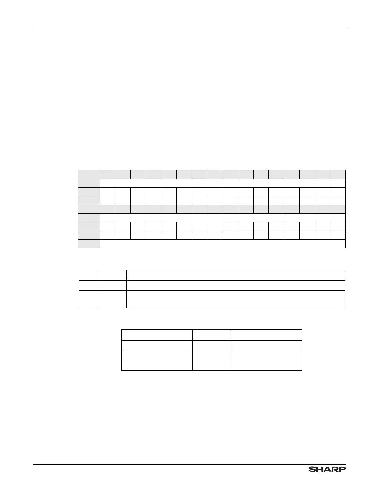
Table 13-43. USBPRE Register
BIT 31 30 29 28 27 26 25 24 23 22 21 20 19 18 17 16
FIELD ///
RESET 0000000000000000
RW RO RO RO RO RO RO RO RO RO RO RO RO RO RO RO RO
BIT 15 14 13 12 11 10 9 8 7 6 5 4 3 2 1 0
FIELD /// USBDIV
RESET 0000000000000000
RW RO RO RO RO RO RO RO RO RW RW RW RW RW RW RW RW
ADDR 0xFFFE2000 + 0x4C
Table 13-44. USBPRE Fields
BITS NAME DESCRIPTION
31:8 /// Reserved Reading returns 0. Write the reset value.
7:0 USBDIV
USB Clock Divisor Program with the clock source divisor for the USB Clock
prescaler (Table 13-45).
Table 13-45. USBPRE Register Values
USBDIV DIVISOR ƒ(ADC)
00000000 (default) 1 ƒ(clock source)
00000001 2 ƒ(clock source)/2
00000010 4 ƒ(clock source)/4