LH79524/LH79525 User’s Guide Color Liquid Crystal Display Controller
Version 1.0 4-19
4.5 CLCDC Register Reference
This section contains the register definitions for the CLCDC. ALI registers are found in the
next section.
4.5.1 Enabling the CLCDC
Following reset, the CLCDC Data Clock is gated OFF. Prior to using the CLCDC, it
must be enabled by turning on the LCD Data Clock in the PCLKCTRL1 register of the
Reset, Clock, and Power Controller block (see Section 13.2.2.10). Registers cannot
be programmed until the LCD Data Clock is enabled.
4.5.2 CLCDC Memory Map
The base address for the CLCDC is: 0xFFFF4000
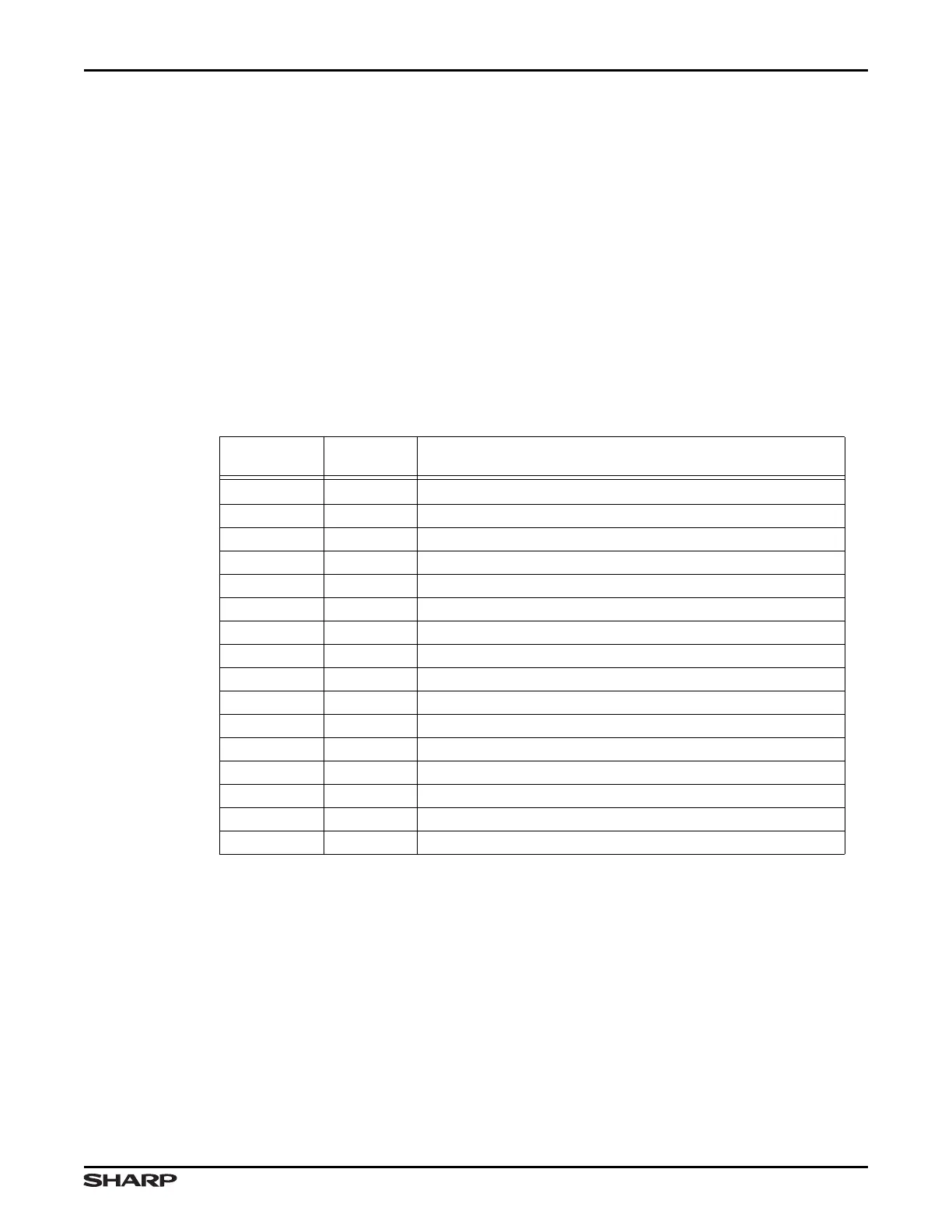
Table 4-13. CLCDC Register Summary
ADDRESS
OFFSET
NAME DESCRIPTION
0x000
TIMING0
Horizontal Axis Timing Control
0x004 TIMING1 Vertical Axis Timing Control
0x008 TIMING2 Clock and Signal Polarity Control Register
0x00C /// Reserved — Do not access
0x010 UPBASE Upper Panel Frame Buffer Base Address Register
0x014 LPBASE Lower Panel Frame Buffer Base Address Register
0x018 INTREN Interrupt Enable Register
0x01C CTRL Panel Parameters, Panel Power, and Control
0x020 STATUS Raw Interrupt Status Register
0x024 INTERRUPT Masked Interrupt Status Register
0x028 INTCLR Interrupt Clear Register
0x02C UPCURR Upper Panel Frame Buffer Current Address Register
0x030 LPCURR Lower Panel Frame Buffer Current Address Register
0x034 - 0x1FC /// Reserved — Do not access
0x200 - 0x3FC PALETTE 256 × 16-bit Color Palette Register. Palette is addressed at 32 bits.
0x400 - 0x7FF /// Reserved — Do not access