Color Liquid Crystal Display Controller LH79524/LH79525 User’s Guide
4-38 Version 1.0
4.5.4 ALI Register Reference
The base address for the ALI is: 0xFFFE4000
Locations at offsets 0x010 through 0xFFF are reserved and must not be used during
normal operation.
4.5.5 ALI Memory Map
4.5.6 ALI Register Descriptions
4.5.6.1 Setup Register (ALISETUP)
The ALISETUP Register puts the ALI into Bypass Mode and configures the basic behavior
of the control signals.
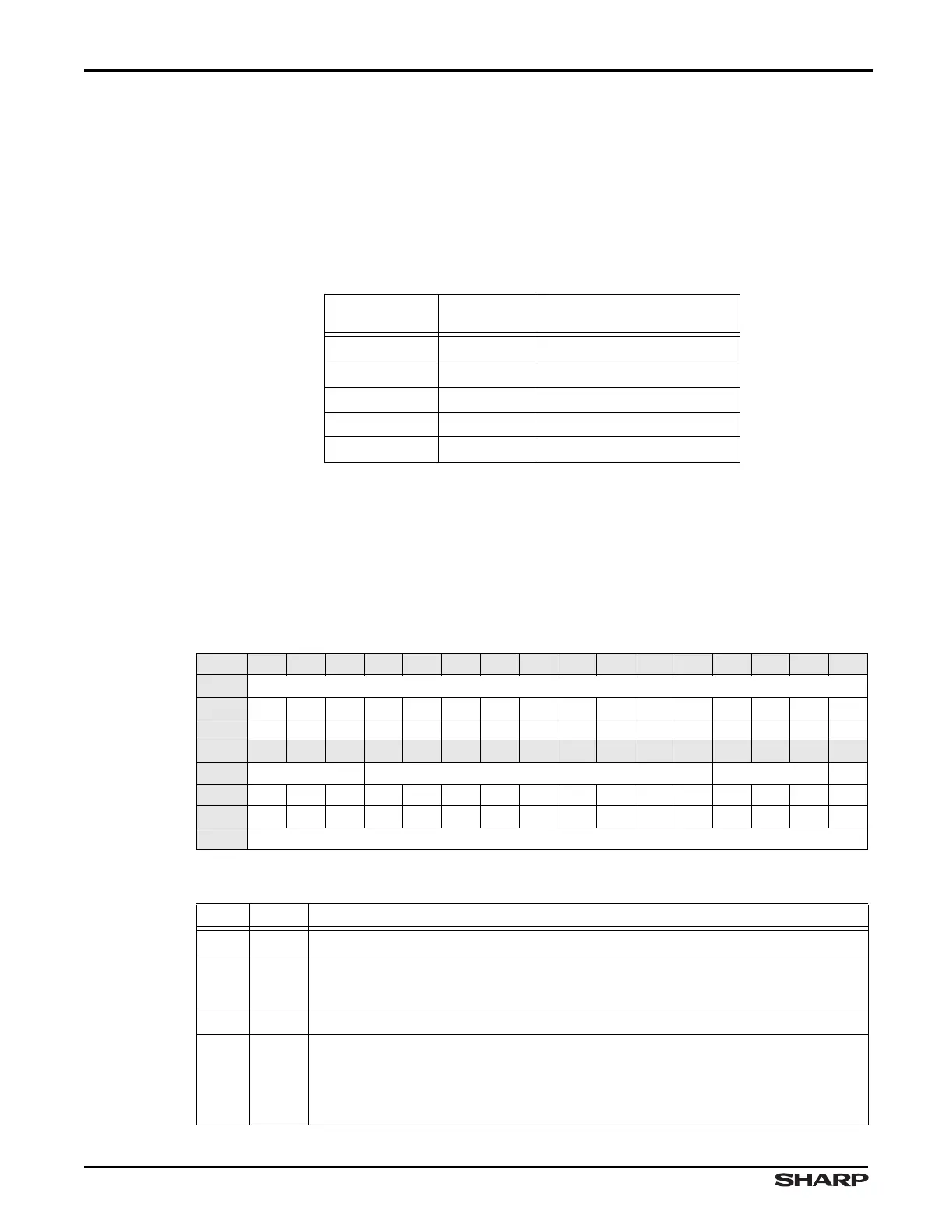
Table 4-42. ALI Register Summary
ADDRESS
OFFSET
NAME DESCRIPTION
0x000 ALISETUP ALI Setup Register
0x004 ALICTRL ALI Control Register
0x008 ALITIMING1 ALI Timing Register 1
0x00C ALITIMING2 ALI Timing Register 2
0x010 - 0xFFF /// Reserved — Do not access
Table 4-43. ALISETUP Register
BIT 31 30 29 28 27 26 25 24 23 22 21 20 19 18 17 16
FIELD ///
RESET 0000000000000000
RW RO RO RO RO RO RO RO RO RO RO RO RO RO RO RO RO
BIT 15 14 13 12 11 10 9 8 7 6 5 4 3 2 1 0
FIELD /// PPL /// CR
RESET 0000000000001100
RW RO RO RO RW RW RW RW RW RW RW RW RW RO RO RO RW
ADDR 0xFFFE4000 + 0x000
Table 4-44. ALISETUP Fields
BITS NAME DESCRIPTION
31:13
/// Reserved Reading returns 0. Write the reset value.
12:4 PPL
Pixels Per Line
PPL = (Actual Pixels per line) – 1.
3:1 /// Reserved Reading returns 0. Write the reset value.
0CR
Conversion Mode Select This bit selects the conversion mode for the ALI.
Change the ALI mode only when the CLCDC is disabled.
1 = ALI Mode
0 = Bypass Mode