LH79524/LH79525 User’s Guide I/O Configuration
Version 1.0 11-3
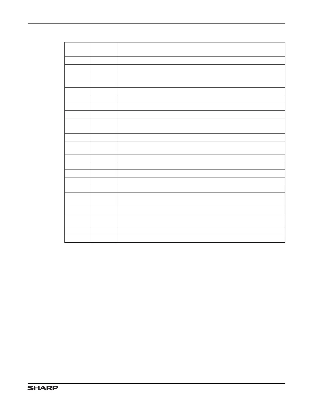
0x70 MUXCTL15 Muxing Control 15 For Pin nBLE0/PM4
0x74 RESCTL15 Resistor Control 15 Assignment for pin nBLE0/PM4
0x78 /// Reserved Do not access
0x7C /// Reserved Do not access
0x80 /// Reserved Do not access
0x84 RESCTL17 Resistor Control 17 Assignment for pin SDCLK
0x88 /// Reserved Do not access
0x8C /// Reserved Do not access
0x90 MUXCTL19 Muxing Control 19 For pins From PE7/nWAIT/nDEOT to PL5/D29
0x94 RESCTL19 Resistor Control 19 Assignment for pins from PE7/nWAIT/nDEOT to PL5/D29
0x98 MUXCTL20 Muxing Control 20 For pins from PE2/LCDPS to PF6/LCDEN/LCDSPL
0x9C RESCTL20
Resistor Control 20 Assignment for pins from PE2/LCDPS to
PF6/LCDEN/LCDSPL
0xA0 MUXCTL21 Muxing Control 21 For pins from PF5/LCDVD11 to PF2/LCDVD8
0xA4 RESCTL21 Resistor Control 21 Assignment for pins from PF5/LCDVD11 to PF2/LCDVD8
0xA8 MUXCTL22 Muxing Control 22 For pins from PF1/LCDVD7 to PG2/LCDVD0
0xAC RESCTL22 Resistor Control 22 Assignment for pins from PF1/LCDVD7 to PG2/LCDVD0
0xB0 MUXCTL23 Muxing Control 23 For pins from PG1/ETHERTXCLK to PH2/ETHERRXCLK
0xB4 RESCTL23
Resistor Control 23 Assignment for pins from PG1/ETHERTXCLK to
PH2/ETHERRXCLK
0xB8 MUXCTL24 Muxing Control 24 For pins from PH1/ETHERRXDV to PI3/ETHERCRS
0xBC RESCTL24
Resistor Control 24 Assignment for pins from PH1/ETHERRXDV to
PI3/ETHERCRS
0xC0 MUXCTL25 Muxing Control 25 For pins from AN6/PJ7/INT7 to AN3/LR/Y-/PJ0
0xC4 /// Reserved Do not access
Table 11-1. IOCON Register Summary
ADDRESS
OFFSET
NAME DESCRIPTION