LH79524/LH79525 User’s Guide Universal Serial Bus Device
Version 1.0 17-9
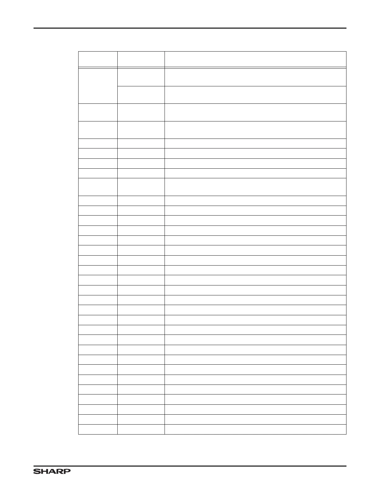
0x058
OUTCOUNT0
Number of received bytes in Endpoint 0 FIFO. (INDEX register
set to select Endpoint 0)
OUTCOUNT1
Number of bytes in OUT endpoint FIFO (lower byte). (INDEX reg-
ister set to select Endpoints 1 – 3)
0x05C OUTCOUNT2
Number of bytes in OUT endpoint FIFO (upper byte). (INDEX reg-
ister set to select Endpoints 1 – 3 only)
0x060 to
0x07F
/// Reserved — Do not access
0x080 EP0FIFO FIFO for Endpoint 0.
0x090 EP1FIFO FIFO for Endpoint 1.
0x0A0 EP2FIFO FIFO for Endpoint 2.
0x0B0 EP3FIFO FIFO for Endpoint 3.
0x0C0 to
0x1FF
/// Reserved — Do not access
0x200 INTR Indicates pending DMA interrupts
0x204 CNTL1 DMA Channel 1 Control
0x208 ADDR1 DMA Channel 1 AHB Memory Address (32 bits)
0x20C COUNT1 DMA Channel 1 Byte Count (32 bits)
0x210 /// Reserved — Do not access
0x214 CNTL2 DMA Channel 2 Control
0x218 ADDR2 DMA Channel 2 AHB Memory Address (32 bits)
0x21C COUNT2 DMA Channel 2 Byte Count (32 bits)
0x220 /// Reserved — Do not access
0x224 CNTL3 DMA Channel 3 Control
0x228 ADDR3 DMA Channel 3 AHB Memory Address (32 bits)
0x22C COUNT3 DMA Channel 3 Byte Count (32 bits)
0x230 /// Reserved — Do not access
0x234 CNTL4 DMA Channel 4 Control
0x238 ADDR4 DMA Channel 4 AHB Memory Address (32 bits)
0x23C COUNT4 DMA Channel 4 Byte Count (32 bits)
0x240 /// Reserved — Do not access
0x244 CNTL5 DMA Channel 5 Control
0x248 ADDR5 DMA Channel 5 AHB Memory Address (32 bits)
0x24C COUNT5 DMA Channel 5 Byte Count (32 bits)
0x250 /// Reserved — Do not access
0x254 CNTL6 DMA Channel 6 Control
0x258 ADDR6 DMA Channel 6 AHB Memory Address (32 bits)
0x25C COUNT6 DMA Channel 6 Byte Count (32 bits)
Table 17-3. USB Register Summary (Cont’d)
ADDRESS
OFFSET
NAME DESCRIPTION