6.8.1 Storage
Attribute
Control Registers
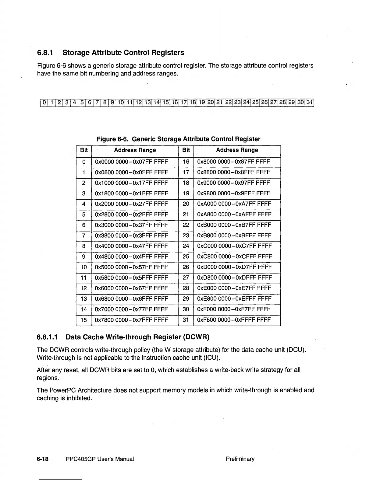
Figure 6-6 shows a generic storage attribute control register. The storage attribute control registers
have the same bit numbering and address ranges.
I 0
11
I
21
31
41
51
61
71
81
91
1
0 111112113114115116117118119120 121122123124125126127128129130 1
31
1
Figure 6-6. Generic Storage Attribute Control Register
Bit
Address Range
Bit Address Range
0
OxOOOO
0000
-Ox07FF
FFFF 16
Ox8000 0000
-Ox87FF
FFFF
1
Ox0800 0000 -OxOFFF FFFF
17
Ox8800 0000
-Ox8FFF
FFFF
2
Ox1000 0000
-Ox17FF
FFFF 18
Ox9000 0000
-Ox97FF
FFFF
3
Ox1800 0000 -Ox1 FFF FFFF 19
Ox9800 0000
-Ox9FFF
FFFF
4
Ox2000 0000
-Ox27FF
FFFF
20
OxAOOO
0000-OxA7FF
FFFF
5
Ox2800 0000
-Ox2FFF
FFFF
21
OxA800 0000
-OxAFFF
FFFF
6
Ox3000 0000
-Ox37FF
FFFF
22
OxBOOO
0000
-OxB7FF
FFFF
7
Ox3800 0000
-Ox3FFF
FFFF
23
OxB800 0000
-OxBFFF
FFFF
8
Ox4000
0000-Ox47FF
FFFF
24
OxCOOO
0000
-OxC7FF
FFFF
9
Ox4800 0000
-Ox4FFF
FFFF 25
OxC800 0000
-OxCFFF
FFFF
10
Ox5000 0000
-Ox57FF
FFFF 26
OxDOOOOOOO-OxD7FFFFFF
11
Ox5800 0000
-Ox5FFF
FFFF
27
OxD800 0000
-OxDFFF
FFFF
12
Ox6000 0000
-Ox67FF
FFFF
28
OxEOOO
0000
-OxE7FF
FFFF
13
Ox6800 0000
-Ox6FFF
FFFF
29
OxE800 0000
-OxEFFF
FFFF
14
Ox7000 0000
-Ox77FF
FFFF 30
OxFOOO
0000
-OxF7FF
FFFF
15
Ox7800 0000
-Ox7FFF
FFFF
31
OxF800 0000
-OxFFFF
FFFF
6.8.1.1
Data Cache Write-through Register
(OCWR)
The DCWR controls write-through policy (the W storage attribute) for the data cache unit (DCU).
Write·through is not
applicable to the instruction cache unit (ICU).
After any reset, all DCWR bits are set to
0,
which establishes a write-back write strategy for all
regions.
The PowerPC Architecture does not support memory
models in which write-through is enabled and
caching is inhibited.
6-18 PPC405GP User's Manual
Preliminary

 Loading...


