EN
DN
RN
0
~
i-
i-
i-
13
1
130
241
23 16
1
15
111
1
0
81
7
211
10
I
t
t
BN
FN
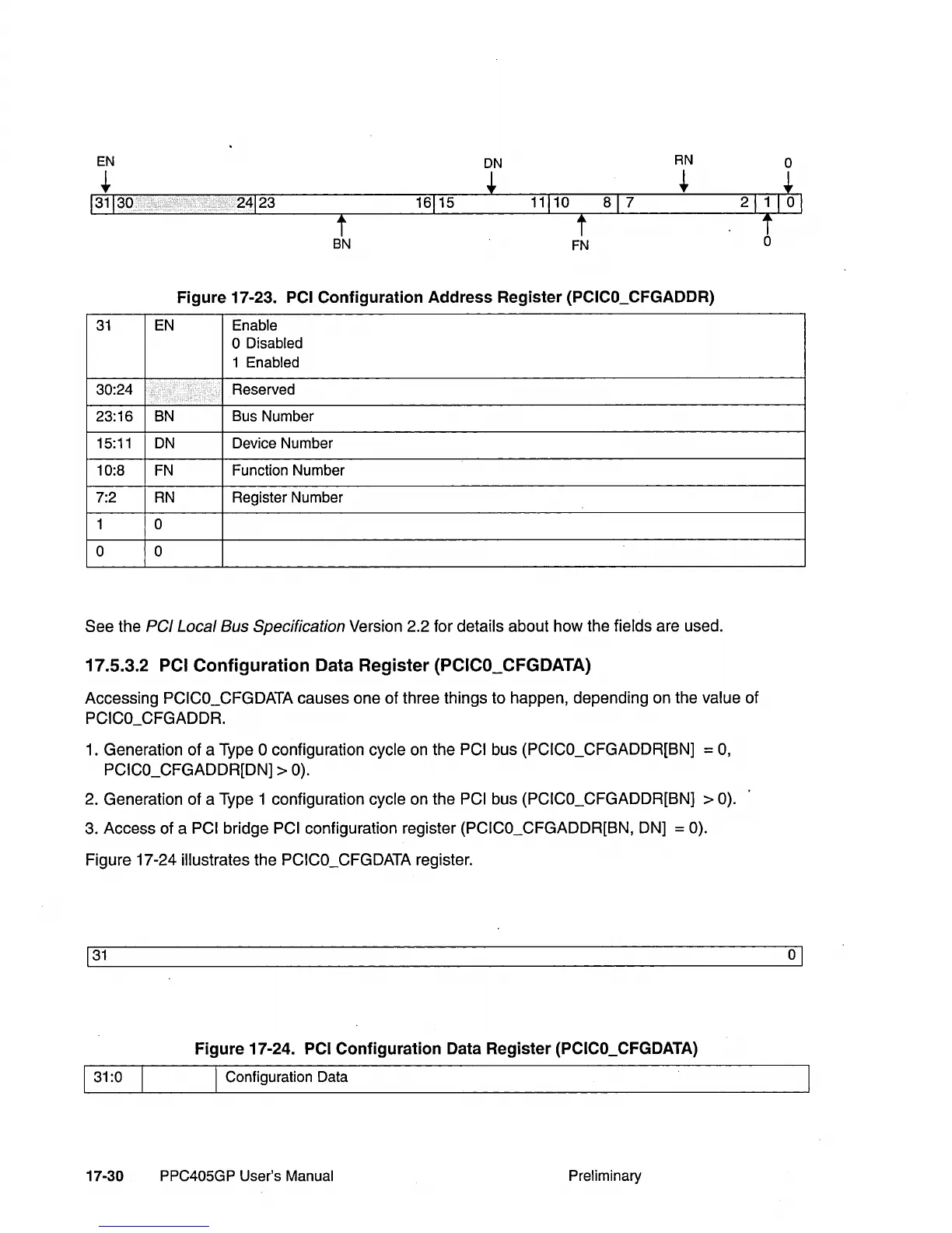
Figure 17-23.
PCI
Configuration Address Register (PCICO_CFGADDR)
31
EN
Enable
o Disabled
1 Enabled
30:24 Reserved
23:16 BN
Bus Number
15:11
DN
Device Number
10:8
FN
Function Number
7:2
RN
Register Number
1
0
0 0
See the PCI Local Bus Specification Version 2.2 for details about how the fields are used.
17.5.3.2
PCI
Configuration
Data Register (PCICO_CFGDATA)
Accessing PCICO_CFGDATA causes one of three things to happen, depending on the value of
PCICO_CFGADDR.
1.
Generation of a Type ° configuration cycle
on
the PCI bus (PCICO_CFGADDR[BN] =
0,
PCICO_CFGADDR[DN] > 0).
2.
Generation of a Type 1 configuration cycle on the PCI bus (PCICO_CFGADDR[BN] > 0).
3.
Access of a PCI bridge PCI configuration register (PCICO_CFGADDR[BN, DN] = 0).
Figure 17-24 illustrates the PCICO_CFGDATA register.
1
31
Figure 17-24. PCI Configuration Data Register (PCICO_CFGDATA)
I 31:0
I Configuration Data
17-30 PPC405GP User's Manual
Preliminary
f
0
01