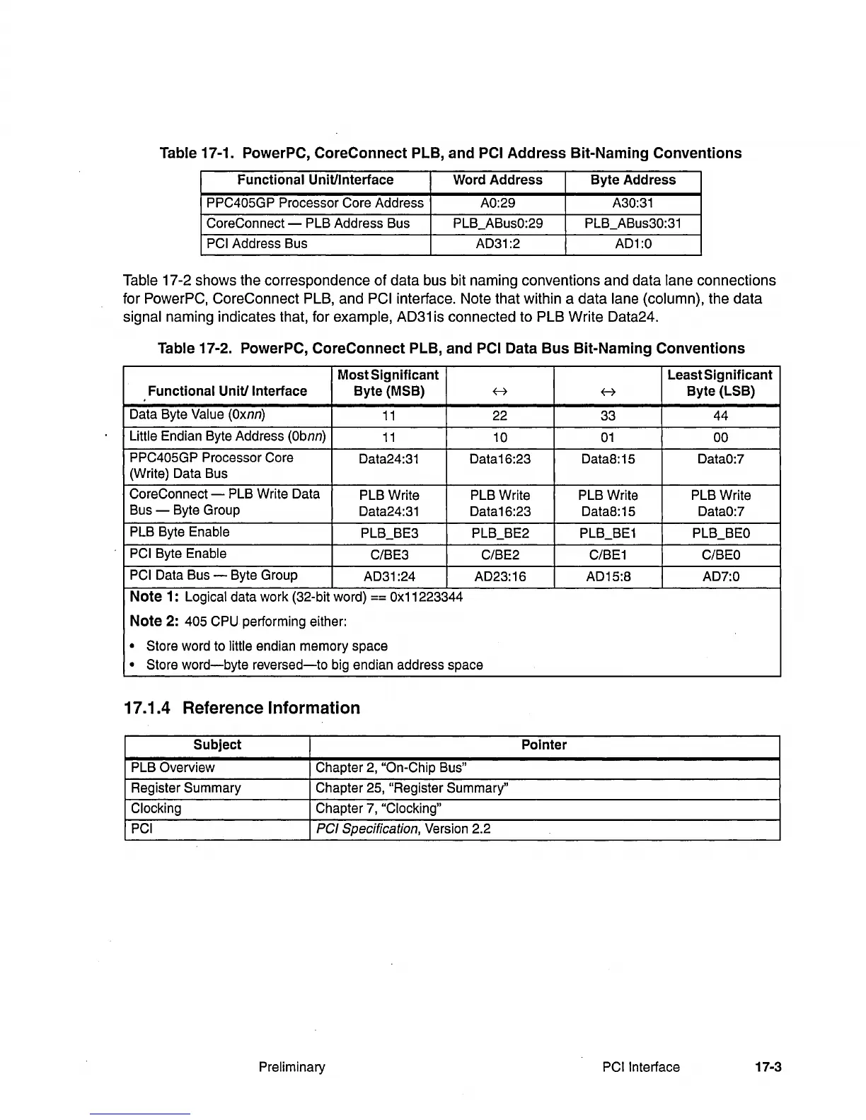
Table 17-1. PowerPC, CoreConnect PLB, and
PCI
Address Bit-Naming Conventions
Functional
Unit/Interface Word
Address
Byte
Address
PPC405GP Processor Core Address
AO:29
A30:31
CoreConnect - PLB Address Bus PLB_ABusO:29 PLB_ABus30:31
PCI Address Bus AD31:2 AD1:0
Table 17-2 shows the correspondence of data bus bit naming conventions and data lane connections
for PowerPC, CoreConnect PLB, and
PCI interface. Note that within a data lane (column), the data
signal naming indicates that, for example, AD31 is connected to PLB Write Data24.
Table 17-2. PowerPC, CoreConnect PLB, and
PCI
Data Bus Bit-Naming Conventions
Most
Significant
LeastSignificant
Functional
Unit/Interface
Byte
(MSB)
f-7
f-7
Byte
(LSB)
Data Byte Value
(Oxnn)
11
22
33
44
Little Endian Byte Address
(Obnn)
11
10
01
00
PPC405GP Processor Core
Data24:31
Data16:23
Data8:15 DataO:7
(Write) Data Bus
CoreConnect - PLB Write Data
PLB Write PLB Write PLB Write PLB Write
Bus - Byte Group
Data24:31
Data16:23 Data8:15
DataO:7
PLB Byte Enable
PLB_BE3 PLB_BE2 PLB_BE1 PLB_BEO
PCI
Byte Enable
C/BE3 C/BE2 C/BE1
C/BEO
PCI
Data Bus - Byte Group
AD31:24 AD23:16 AD15:8 AD7:0
Note 1: Logical data work (32-bit word)
==
0)(11223344
Note
2:
405 CPU performing either:
.
Store word to little endian memory space
.
Store
word-byte
reversed-to
big end ian address space
17.1.4 Reference Information
Subject
Pointer
PLB Overview Chapter
2,
"On-Chip Bus"
Register Summary Chapter 25, "Register Summary"
Clocking
Chapter
7,
"Clocking"
PCI
PCI Specification, Version 2.2
Preliminary
PCI Interface 17-3

 Loading...


