10.22 Watchdog Timer Interrupt
For a general description of the PPC405GP timer facilities, see Chapter 11, "Timer Facilities:' The
watchdog timer (WDT) is described in
"Watchdog Timer" on page 11-6.
If the
WDT
interrupt is enabled by TCR[WIE] and MSR[CE], the PPC405GP initiates a
WDT
interrupt
after detecting the first
WDT
time-out. First time-out is detected when, at the beginning
of
a clock
cycle, TSR[WIS]
= 1. (This occurs on the second cycle after the
O~
1 transition of the appropriate
time-base bit
while TSR[ENW] = 1 and TSR[WIS] = 0.) The PPC405GP immediately takes the
interrupt. The address of the next
sequential instruction is saved in SRR2; simultaneously, the
contents of the MSR are written into SRR3 and the MSR is written with the
values shown in
Table 10-20. The high-order 16 bits of the program counter are then written with the contents of the
EVPR and the low-order 16 bits of the program counter are written with Ox1020. Interrupt processing
begins at the address in the program counter.
To
clear the
WDT
interrupt, the interrupt handling routine must clear the
WDT
interrupt bit TSR[WIS].
Clearing
is done by writing a word to TSR (using
mtspr),
with a 1 in any bit position that is to be
cleared and 0 in all other bit positions. The data written to the status register is not direct data, but a
mask; a 1 causes the bit to be
cleared, and a 0 has no effect.
Executing the return from
critical interrupt instruction
(rfci)
restores the contents of the program
counter and the MSR
from SRR2 and SRR3, respectively, and the PPC405GP resumes execution at
the contents of the program counter.
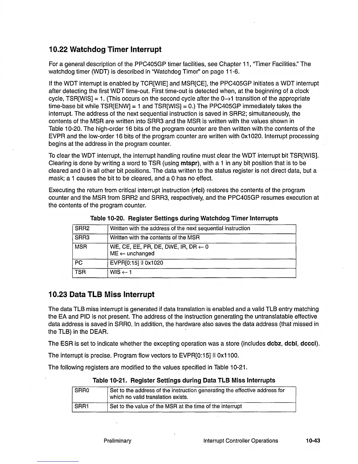
Table 10-20.
Register
Settings
during
Watchdog
Timer
Interrupts
SRR2
Written
with
the
address of
the
next
sequential instruction
SRR3
Written
with
the
contents
of
the
MSR
MSR
WE,
CE,
EE,
PR,
DE,
OWE,
IR,
DR
~
0
ME
~
unchanged
PC
EVPR[O:15]
II
Ox1020
TSR
WIS~1
10.23 Data TLB Miss Interrupt
The data TLB miss interrupt is generated if data translation is enabled and a valid
TLB
entry matching
the EA and
PID is not present. The address of the instruction generating the untranslatable effective
data address is saved in
SRRO. In addition, the hardware also saves the data address (that'missed in
the TLB)
in
the DEAR. '
The
ESR is set to indicate whether the excepting operation was a store (includes
dcbz,
dcbi,
dccci).
The interrupt is precise. Program flow vectors to EVPR[0:15]
II
Ox11
00.
The following registers are modified to the values specified in Table 10-21.
Table
10-21.
Register
Settings
during
Data
TLB
Miss
Interrupts
SRRO
Set
to
the
address
of
the
instruction generating
the
effective address
for
which
no
valid translation
exists.
SRR1
Set
to
the
value
of
the
MSR
at
the
time
of
the
interrupt
Preliminary
Interrupt Controller
Operations 10-43