references or cache instructions.The fields DBCR1 [01 R], [D2R] and DBCR[D1 W], [D2W] control the
DAC-read and DAC-write debug events,
respectively.
Addresses
in
the DAC registers specify exact byte EAs for DAC debug events. However, one may
want to take a debug
event on any byte within a halfword (ignore the least significant bit (L8b) of the
DAC), on any byte within a word (ignore the two L8bs of DAC),
or
on any byte within eight words
(ignore four L8bs of DAC). DBCR1
[018,
028]
control the addressing options.
Errors
related to execution of storage reference
or
cache instructions prevent
DAC
debug events.
1
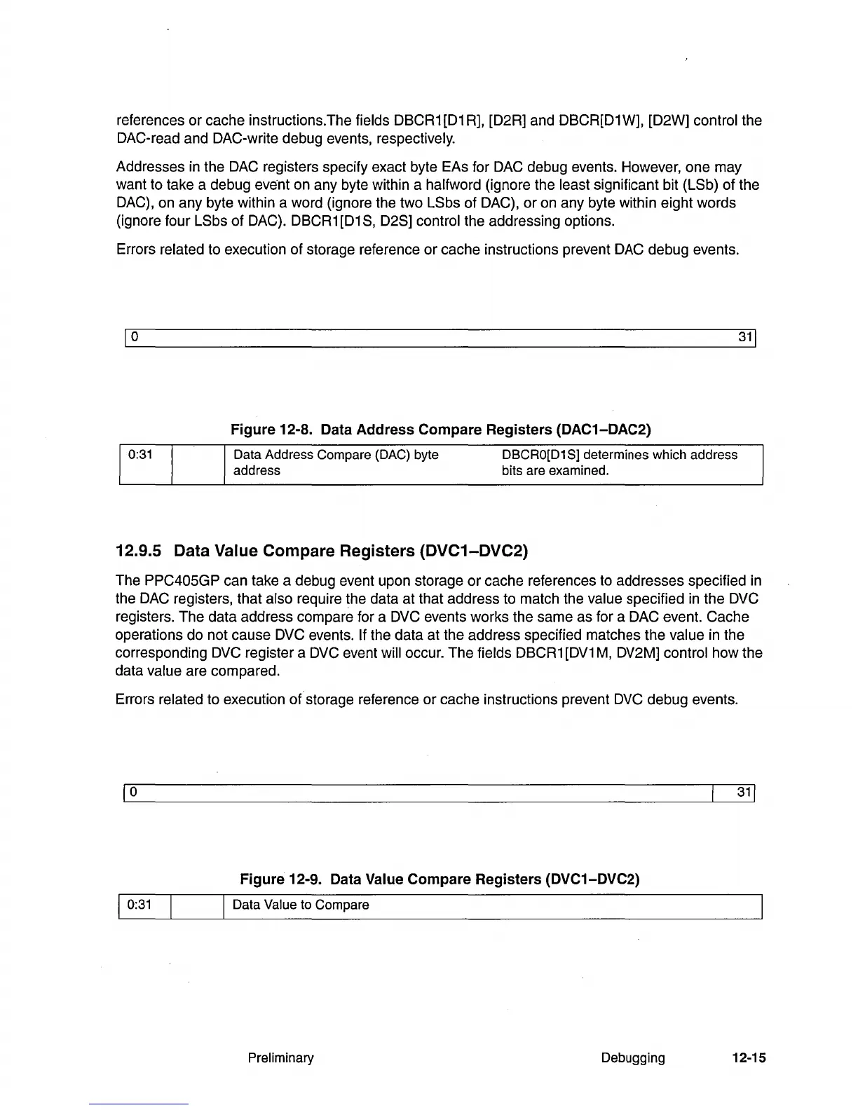
0
Figure 12-8. Data Address Compare Registers (DAC1-DAC2)
Data Address Compare (DAC) byte
address
DBCRO[D1 S] determines which address
bits are examined.
12.9.5 Data Value Compare Registers (DVC1-DVC2)
The PPC405GP can take a debug event upon storage
or
cache references to addresses specified
in
the DAC registers, that also require the data at that address to match the value specified
in
the DVC
registers. The data address compare for a
DVC
events works the same as for a DAC event. Cache
operations do not cause
DVC events. If the data at the address specified matches the value
in
the
corresponding
DVC register a DVC event will occur. The fields DBCR1
[DV1
M,
DV2M]
control how the
data
value are compared.
Errors
related to execution of storage reference
or
cache instructions prevent
DVC
debug events.
1
0
31
1
Figure 12-9. Data Value Compare Registers (DVC1-DVC2)
I 0:31
Data Value to Compare
Preliminary Debugging 12-15