7.3 External Clock Strapping Setup
The PPC405GP configures its clocking based on strapping resistors connected
to
module I/O pins.
The state of the strapping pins is stored
in
the Chip Pin Strapping Register (CPCO_PSR) upon power-
on
or
system reset. Software can use this read-only register to determine clock strapping values.
Table
7-1
indicates which CPCO_PSR fields are assigned to clocking functions and how they are
encoded.
See Chapter
9,
"Pin Strapping and Sharing" for a more information and a complete list of
strapping
values.
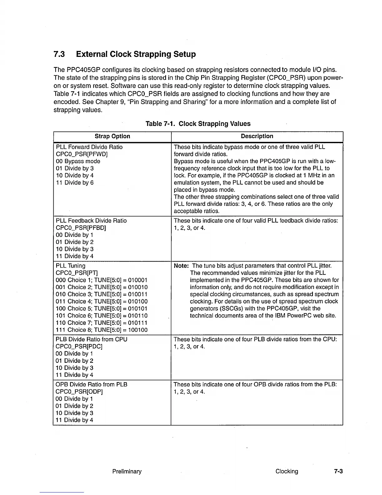
Table 7-1.
Clock
Strapping
Values
Strap
Option
Description
PLL Forward Divide Ratio These bits indicate bypass mode or one
of
three valid PLL
CPCO_PSR[PFWD] forward divide ratios.
00 Bypass mode
Bypass mode is useful when the PPC405GP is run with a low-
01
Divide by 3 frequency reference clock input that is too low for the PLL to
10 Divide by 4 lock. For example, if the PPC405GP is clocked at 1 MHz
in
an
11
Divide by 6
emulation system, the PLL cannot be used and should be
placed
in
bypass mode.
The other three strapping combinations
select one of three valid
PLL forward divide ratios:
3,
4,
or
6.
These ratios are the only
acceptable
ratios.
PLL Feedback Divide Ratio These bits indicate one of four
valid PLL feedback divide ratios:
CPCO_PSR[PFBD]
1,2,3,
or
4.
00 Divide by 1
01
Divide by 2
10 Divide by 3
11
Divide by 4
PLL Tuning Note: The tune bits adjust parameters that
control PLL jitter.
CPCO_PSR[PT]
The recommended values minimize jitter for the PLL
000 Choice
1;
TUNE[5:0] = 010001
implemented
in
the PPC405GP. These bits are shown for
001
Choice
2;
TUNE[5:0] = 010010
information only, and do not require modification except
in
010 Choice
3;
TUNE[5:0] = 010011
special clocking circumstances, such as spread spectrum
011
Choice
4;
TUNE[5:0] = 010100
clocking. For details on the use of spread spectrum clock
100
Choice
5;
TUNE[5:0] = 010101 generators (SSCGs) with the PPC405GP, visit the
101
Choice
6;
TUNE[5:0] = 010110
technical documents area of the IBM PowerPC web site.
110 Choice
7;
TUNE[5:0] = 010111
111
Choice
8;
TUNE[5:0] = 100100
PLB Divide Ratio from CPU These bits indicate one of four PLB divide ratios from the CPU:
CPCO.:...PSR[PDC]
1,2,3,
or
4.
00 Divide by 1
01
Divide by 2
10 Divide by 3
11
Divide by 4
OPB Divide Ratio from PLB These bits indicate one of four OPB divide ratios from the PLB:
CPCO_PSR[ODP]
1,2,3,
or
4.
00 Divide by 1
01
Divide by 2
10 Divide by 3
11
Divide by 4
Preliminary
Clocking
7-3