Chapter
7.
Clocking
Clocking
in
the PPC405GP is highly configurable and supports a wide range of clock ratios on the
internal and external buses.
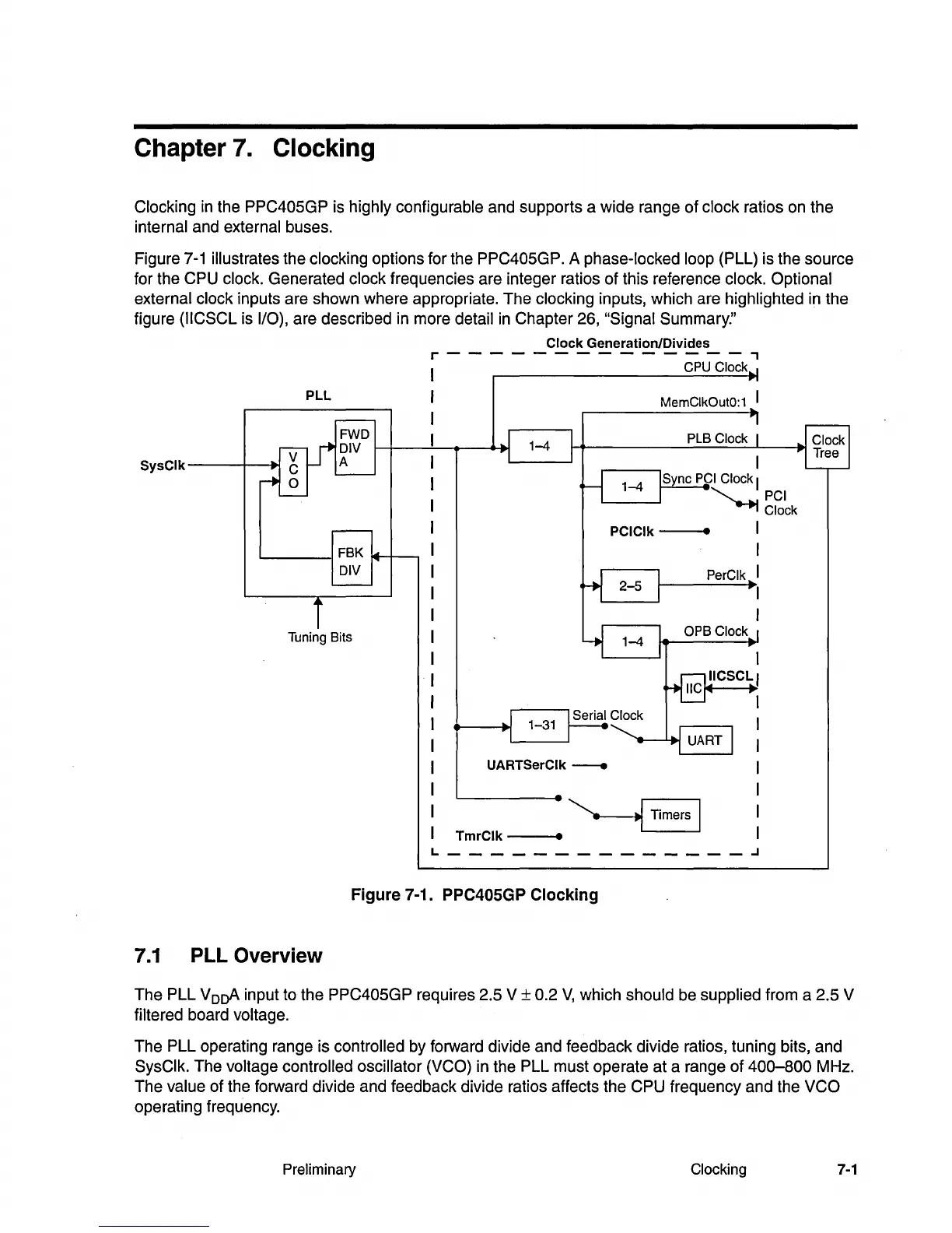
Figure
7-1
illustrates the clocking options for the PPC405GP. A phase-locked loop (PLL) is the source
for the CPU clock. Generated clock frequencies are integer ratios of this reference clock. Optional
external clock inputs are shown where appropriate. The clocking inputs, which are highlighted in the
figure
(IICSCL is
1/0),
are described
in
more detail
in
Chapter 26, "Signal Summary:'
Clock
Generation/Divides
r--------------,
CPU
Clock
PLL
MemClkOutO:
1 I
PLB
Clock
SysClk----+-~
'--
___
I
FBK
DIV
Tuning
Bits
UARTSerClk
---e
TmrClk
----e
~Timersl
______________
.J
Figure
7-1. PPC405GP
Clocking
7.1
PLL Overview
The PLL VDoA input to the PPC405GP requires 2.5 V ± 0.2
V,
which should be supplied from a 2.5 V
filtered board voltage.
The PLL operating range is controlled by forward divide and feedback divide ratios, tuning bits, and
SysClk. The voltage controlled oscillator
(VCO) in the PLL must operate at a range of
400-800
MHz.
The value of the forward divide and feedback divide ratios affects the CPU frequency and the
VCO
operating frequency.
Preliminary Clocking
7-1