Instruction set statements describe the bit patterns that must be shifted into the Instruction Register to
place the chip
in
the various test modes defined by the standard. Instruction set statements also
support descriptions of instructions that are unique to the chip.
The boundary register description
lists each cell
or
shift stage of the Boundary Register. Each cell has
a unique number: the
cell numbered 0 is the closest to the Test Data Out (TDO) pin; the cell with the
highest number is
closest to the Test Data In (TDI) pin. Each cell contains additional information,
including: cell type, logical port associated with the cell, logical function of the cell, safe value, control
cell
number, disable value, and result value.
12.4.3 JTAG Implementation
PPC405GP JTAG interface II0s (TDI, TDO, TMs, TCK, and TRST) are
5V
tolerant and do not contain
internal pull up resistors
..
The optional JTAG instructions, idcode and highz, offer additional JTAG functionality. The idcode
instruction returns the PPC405GP JTAG
ID,
which is unique for each chip version. The highz
instruction disables all chip outputs regardless of whether they are included
in
the JTAG boundary
scan chain.
The PPC405GP provides boundary scan structures on most
I/O signals. However, the following
signals
are excluded because of speed and functional considerations:
• Drvrlnh1
• Drvrlnh2
• PciClk
• Rcvrlnh
•
TestEn
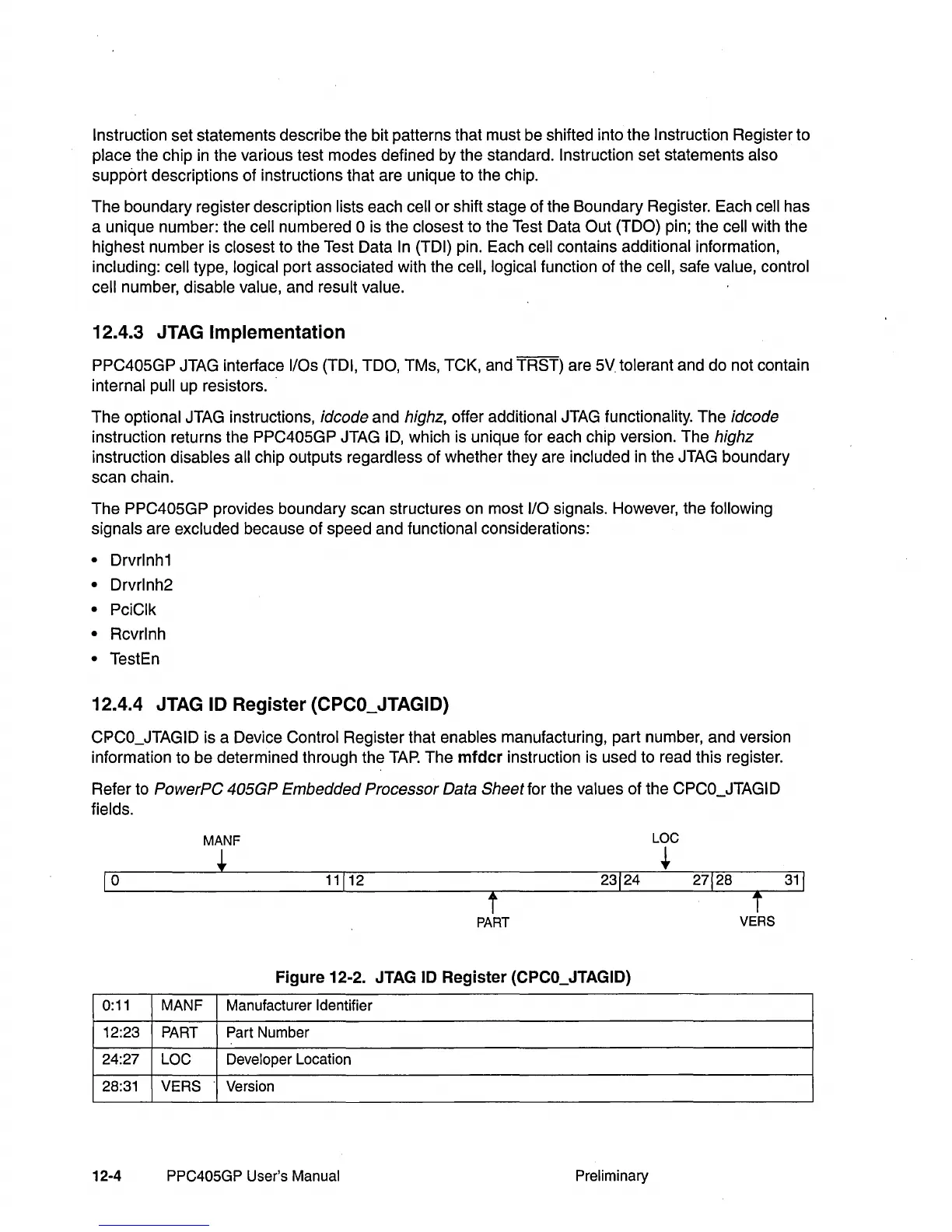
12.4.4 JTAG
10
Register (CPCO_JTAGIO)
CPCO_JTAGID is a Device Control Register that enables manufacturing, part number, and version
information to be determined through the
TAP.
The
mfdcr
instruction is used to read this register.
Refer to
PowerPC 405GP Embedded Processor Data Sheet for the values of the CPCO_JTAGID
fields.
MANF
LOC
...
+
10
11/12
t
23
1
24
27
1
28
f
PART
VERS
Figure 12-2. JTAG
10
Register (CPCO_JTAGIO)
0:11 MANF Manufacturer Identifier
12:23 PART Part Number
24:27
LOC
Developer Location
28:31
VERS Version
12-4
PPC405GP User's Manual
Preliminary
3
1
/