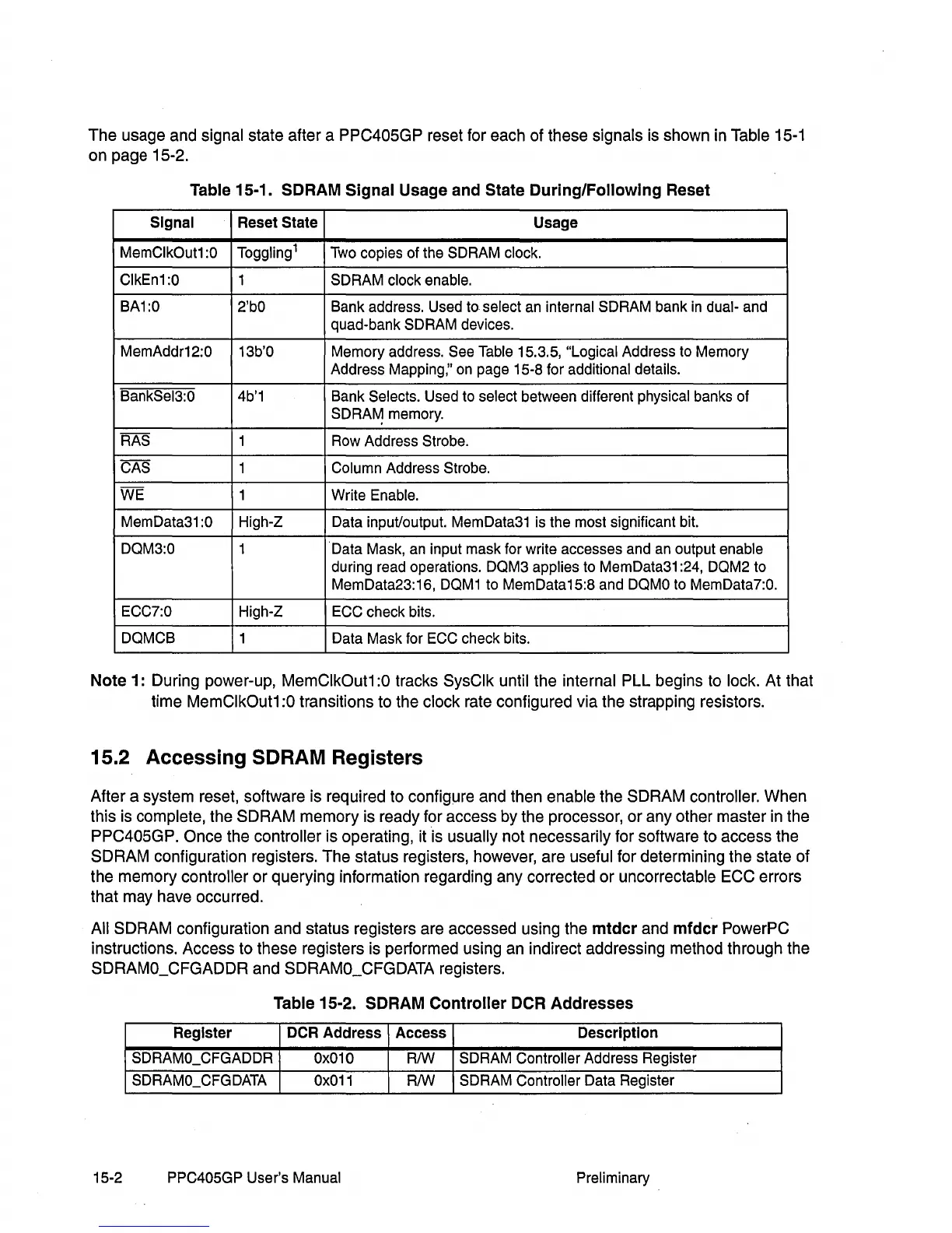
The usage and signal state after a PPC405GP reset for each of these signals is shown in Table
15-1
on page 15-2.
Table 15·1. SDRAM
Signal
Usage and State
During/Following
Reset
Signal
Reset State
Usage
MemClkOut1 :0
Toggling
1
Two
copies of the SDRAM clock.
ClkEn1:0
1 SDRAM clock enable.
BA1:0
2'bO
Bank address. Used to select an internal SDRAM bank
in
dual- and
quad-bank
SDRAM devices.
MemAddr12:0
13b'0 Memory address. See Table 15.3.5, "Logical Address to Memory
Address Mapping," on page 15-8 for additional details.
BankSel3:0
4b'1
Bank Selects. Used to select between different physical banks of
SDRA~
memory.
RAS 1 Row Address Strobe.
CAS
1 Column Address Strobe.
WE 1
Write Enable.
MemData31
:0 High-Z
Data input/output. MemData31 is the most significant bit.
DOM3:0 1 Data Mask, an input mask for write accesses and an output enable
during read operations.
DOM3 applies to MemData31 :24, DQM2 to
MemData23:16,
DQM1
to MemData15:8 and
DOMO
to MemData7:0.
ECC7:0 High-Z
ECC check bits.
DOMCB 1
Data Mask for ECC check bits.
Note
1: During power-up, MemClkOut1:0 tracks SysClk until the internal PLL begins
to
lock. At that
time
MemClkOut1:0 transitions to the clock rate configured via the strapping resistors.
15.2 Accessing SDRAM Registers
After a system reset, software is required to configure and then enable the SDRAM controller. When
this is
complete, the SDRAM memory is ready for access by the processor, or any other master
in
the
PPC405GP.
Once the controller is operating, it is usually not necessarily for software to access the
SDRAM configuration registers. The status registers, however, are useful for determining the state of
the memory
controller or querying information regarding any corrected or uncorrectable ECC errors
that may have occurred.
All SDRAM configuration and status registers are accessed using the
mtdcr
and
mfdcr
PowerPC
instructions. Access to these registers is performed using an indirect addressing method through the
SDRAMO_CFGADDR and SDRAMO_CFGDATA registers.
Table 15·2. SDRAM
Controller
OCR
Addresses
Register
OCR
Address
Access
Description
SDRAMO_CFGADDR Ox010
RIW
SDRAM Controller Address Register
SDRAMO_CFGDATA
Ox011
RIW
SDRAM Controller Data Register
15-2
PPC405GP User's Manual Preliminary