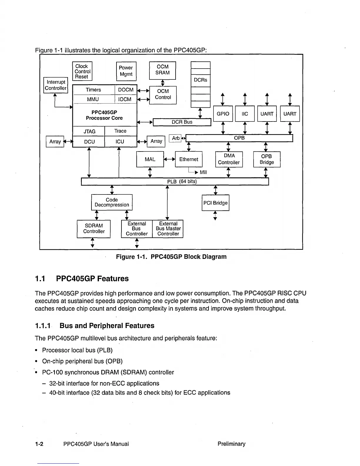
Figure
1-1
illustrates the logical organization of the PPG405GP:
PPC405GP
Processor Core
JTAG
Trace
DCU ICU
DCRs
Figure
1-1. PPC405GP
Block
Diagram
1.1
PPC405GP Features
The PPG405GP provides high performance and low power consumption. The PPG405GP RISG GPU
executes at sustained speeds approaching one cycle per instruction. On-chip instruction and data
caches reduce chip count and design
complexity in systems and improve system throughput.
1.1.1 Bus and Peripheral Features
The PPG405GP multilevel bus architecture and peripherals feature:
• Processor local bus (PLB)
•
On-chip peripheral bus (OPB)
• PG-100
synchronous DRAM (SDRAM) controller
- 32-bit interface for non-EGG applications
- 40-bit interface (32 data bits and 8 check bits) for
EGG
applications
1-2 PPC405GP User's Manual
Preliminary