clock as a PPC405GP system clock input, as required for synchronous PCI mode, can adversely
affect PPC405GP CPU performance. In some cases, the PPC405GP might not function.
For
example, if the PPC405GP is used
on
a PCI adapter and the PCI expansion bus frequency is
33MHz, the PPC405GP strapping pins can be configured to run the chip at
200 MHz. However, if the
same strapping configuration is used and the PPC405GP is used
in
a system
in
which the PCI
expansion bus frequency is 25 MHZ (an application supported by the PCI specification), the
PPC405GP
would run suboptimally at 150 MHz. Worse problems would be encountered if the PCI
frequency were less than 25 Mhz (the PPC405GP PLL locking frequency).
In
this
appli~ation,
the
PPC405GP might not function. For these reasons, asynchronous
PCI mode is recommended when
the PPC405GP is used in
PCI adapter applications.
Asynchronous PCI mode uses an externally provided PCI clock that does not interact with an on-chip
PLL, so there is no
lower frequency limit imposed by loss of PLL lock. However, the requirements
resulting from the relationship between the synchronous and asynchronous PCI clocks must still be
satisfied.
Note: Satisfying the equation
in
"PCI Clocks" on page 7-8 presents a potential problem. The
strapping pin
selection needed to set an acceptable synchronous PCI clock for a 33 MHz
asynchronous
PCI clock differs from the strapping pin selection for a 66 MHz asynchronous
PCI clock. External logic is required to detect the state of the M66 pin on the PCI adapter
interface and
select appropriate PPC405GP strapping pins during system reset.
7.6 Serial Port Clocking
The two PPC405GP UARTs (serial ports) can be clocked individually, either from an external serial
clock
or
from an internally generated serial clock. The internally generated clock is derived from the
CPU
clock, and is CPU/n, where n ranges from 1 to 32. The divisor n is programmed by setting a
value of 0 to
31
in
CPCO_CRO[UDIV] (see "Chip Control Register 0 (CPCO_CRO)" on page 7-11).
Subsequently, the serial clock input to the UART is further divided
in
the UART
to
generate the
desired
serial data rate (baud rate).
Refer to Chapter 21,
"Serial Port Operations," for more information about choosing CPU clock and
serial input clock divisors.
7.7 Clocking Registers
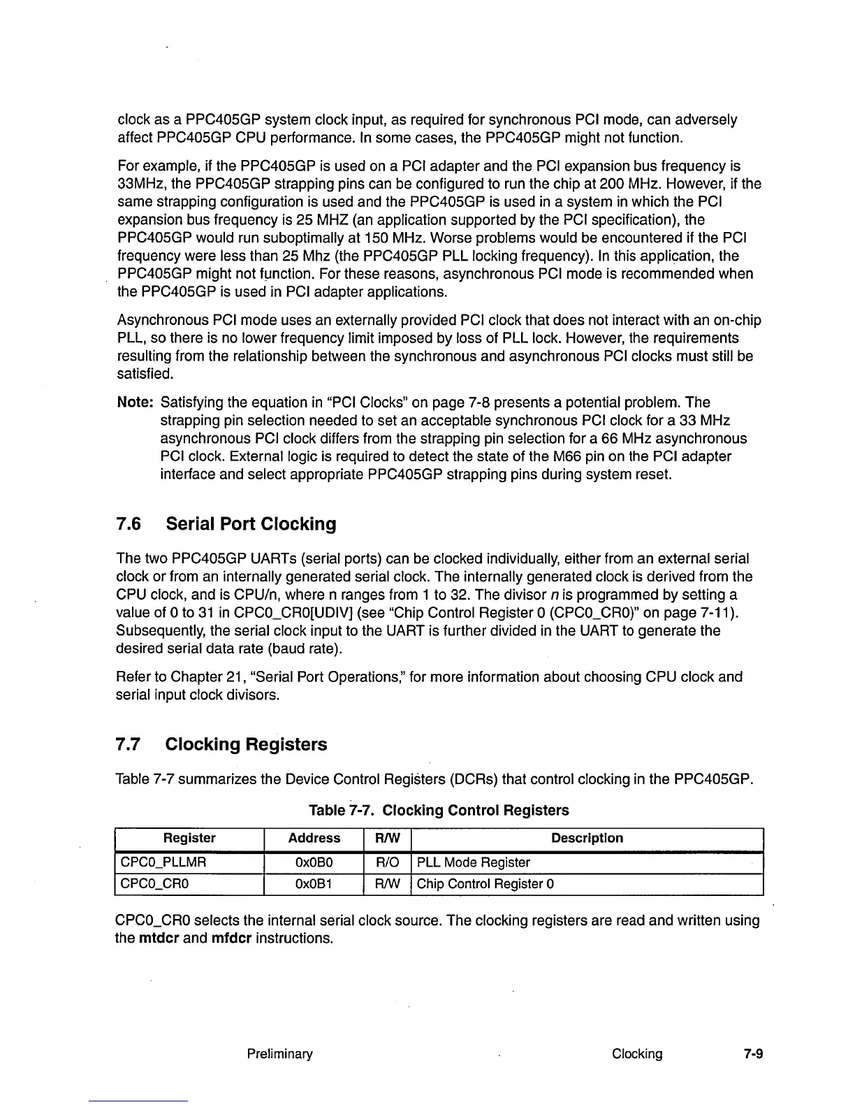
Table 7-7 summarizes the Device Control Registers (DCRs) that control clocking in the PPC405GP.
Table 7-7.
Clocking
Control
Registers
Register
Address
RIW
Description
CPCO_PLLMR
OxOBO
RIO
PLL
Mode
Register
CPCO_CRO
OxOB1
RIW
Chip Control Register 0
CPCO_CRO
selects the internal serial clock source. The clocking registers are read and written using
the
mtdcr
and
mfdcr
instructions.
Preliminary Clocking 7-9