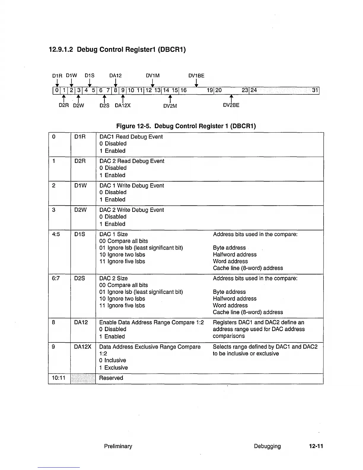
12.9.1.2 Debug Control Register1 (DBCR1)
D1R D1W D1S DA12 DV1M
DV1BE
31
D2S DA12X
DV2M
Figure 12-5. Debug Control Register 1 (DBCR1)
0 D1R
DAC1
Read Debug Event
o Disabled
1 Enabled
1 D2R DAC 2 Read Debug Event
o Disabled
1 Enabled
2
D1W
DAC
1 Write Debug Event
o Disabled
1 Enabled
3 D2W DAC 2 Write Debug Event
o Disabled
1 Enabled
4:5
D1S DAC 1 Size
Address bits used
in
the compare:
00 Compare all bits
01
Ignore Isb (least significant bit) Byte address
10 Ignore two Isbs Halfword address
11
Ignore five Isbs Word address
Cache
line (8-word) address
6:7 D2S
DAC
2 Size Address bits used
in
the compare:
00 Compare all bits
01
Ignore Isb (least significant bit) Byte address
10 Ignore two Isbs Halfword address
11
Ignore five Isbs Word address
Cache
line (8-word) address
8 DA12
Enable Data Address Range Compare 1:2
Registers
DAC1
and DAC2 define an
o Disabled address range used for DAC address
1
Enabled
comparisons
9 DA12X Data Address Exclusive Range Compare Selects range defined by
DAC1
and DAC2
1:2 to be inclusive or
exclusive
o Inclusive
1 Exclusive
10:11
I
Reserved
Preliminary Debugging
12-11