16.4.2 Device-Paced Single Write Transfer
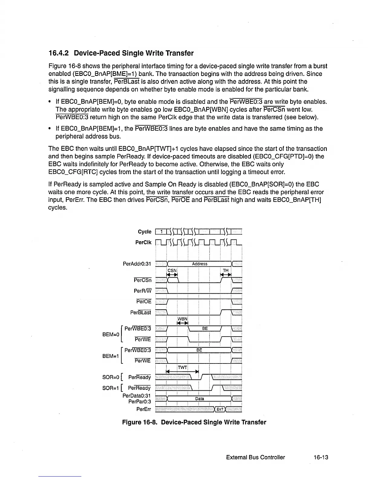
Figure 16-8 shows the peripheral interface timing for a device-paced single write transfer from a burst
enabled (EBCO_BnAP[BME]=1) bank. The transaction begins with the address being driven. Since
this is a
single transfer, PerBLast is also driven active along with the address. At this point the
signalling sequence depends on whether byte enable mode is enabled for the particular bank.
• If EBCO_BnAP[BEM]=O, byte enable mode is disabled and the PerWBEO:3 are write byte enables.
The appropriate write byte enables go low EBCO_BnAP[WBN] cycles after PerCSn went low.
PerWBEO:3
return high on the same PerClk edge that the write data is transferred (see below).
• If
EBCO_BnAP[BEM]=1 , the PerWBEO:3 lines are byte enables and have the same timing as the
peripheral address bus.
The EBC then waits
until EBCO_BnAP[TWT]+ 1 cycles have elapsed since the start of the transaction
and then begins
sample PerReady. If device-paced timeouts are disabled (EBCO_CFG[PTD]=O) the
EBC waits indefinitely for PerReady to become active. Otherwise, the EBC waits
only
EBCO_CFG[RTC] cycles from the start of the transaction until logging a timeout error.
If PerReady is sampled active and Sample On Ready is disabled (EBCO_BnAP[SOR]=O) the EBC
waits one more
cycle. At this paint, the write transfer occurs and the EBC reads the peripheral error
input, PerErr. The EBC then drives PerCSn, PerOE and PerBLast high and waits EBCO_BnAP[TH]
cycles.
Cycle
crntntn)
I I
))r=
PerClk ru)U1U1}rLJlf)w-L
. I .
PerAddrO:31
~
Address C
iCSNi
TH
1+--+1
i ! .
~
PerCSn~
PerRiW
:=j
p
PerOE
:=.J
W
PerBLast
i-Q~L...--~---.;..--,---!rr::J
WBN
[
PerWBEO:3
U
~\I-_B=E:....--,
cJ
BEM=O
PerWE:...J
\
......
-'-~~IC
f
[
perWBEO:3
~==:=:==~BE~======CJ
BEM=1
__
!
PerWE
CJ.
n
I.
;
TWTi
~I
r--":-..--'----i
-'-~~~~\~!I
!\~~
__
~
SOR=O
[
PerReady
SOR=1
[
PerReady
i-~--'--.~\L...--.-J!
I i
c=J
pe~~~~~~~~
q=:::::~D;ata~::::::'d
PerErr
___________
'--!~
Figure
16-8. Device-Paced
Single
Write
Transfer
External Bus Controller 16-13

 Loading...


