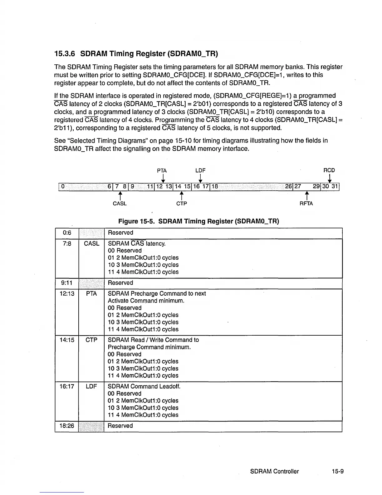
15.3.6 SDRAM Timing Register (SDRAMO_ TR)
The
SDRAM
Timing Register sets the timing parameters for all
SDRAM
memory
banks.
This
register
must
be written prior to setting SDRAMO_CFG[DCE]. If SDRAMO_CFG[DCE]=1 , writes to this
register
appear
to complete, but
do
not affect the contents
of
SDRAMO_ TR.
If the
SDRAM
interface is operated in registered mode, (SDRAMO_CFG[REGE]=1) a programmed
CAS
latency
of
2 clocks (SDRAMO_
TR[CASL]
= 2'b01) corresponds to a registered
CAS
latency
of
3
clocks,
and
a programmed latency of 3 clocks (SDRAMO_ TR[CASL] = 2'b1 0) corresponds
to
a
registered
CAS latency
of
4 clocks. Programming the
CAS
latency to 4 clocks (SDRAMO_
TR[CASL]
=
2'b11), corresponding to a re.gistered
CAS
latency
of
5 clocks, is
not
supported.
See
"Selected Timing Diagrams" on page 15-10 for timing diagrams illustrating
how
the fields in
SDRAMO_
TR
affect the signalling on the
SDRAM
memory
interface.
PTA
LDF
RCD
t
26127 29130
31
1
-*
t
11112131141511617118
...
-*
1
0
t
CASL CTP
RFTA
Figure 15-5. SDRAM
Timing
Register (SDRAMO_ TR)
0:6 Reserved
7:8
CASL SDRAM
CAS
latency.
00
Reserved
01
2 MemClkOut1:0 cycles
10
3 MemClkOut1:0 cycles
11
4 MemClkOut1
:0
cycles
9:11
Reserved
'.
12:13
PTA
SDRAM Precharge Command
to
next
Activate Command minimum.
00
Reserved
01
2 MemClkOut1:0 cycles
10
3 MemClkOut1
:0
cycles
11
4 MemClkOut1
:0
cycles
14:15
CTP
SDRAM
Read
/ Write Command to
Precharge Command minimum.
00
Reserved
01
2 MemClkOut1:0 cycles
10
3 MemClkOut1:0 cycles
11
4 MemClkOut1:0 cycles
16:17
LDF
SDRAM Command Leadoff.
00
Reserved
01
2 MemClkOut1
:0
cycles
10
3 MemClkOut1
:0
cycles
11
4 MemClkOut1
:0
cycles
18:26 ,
....
Reserved
:
SDRAM Controller 15-9