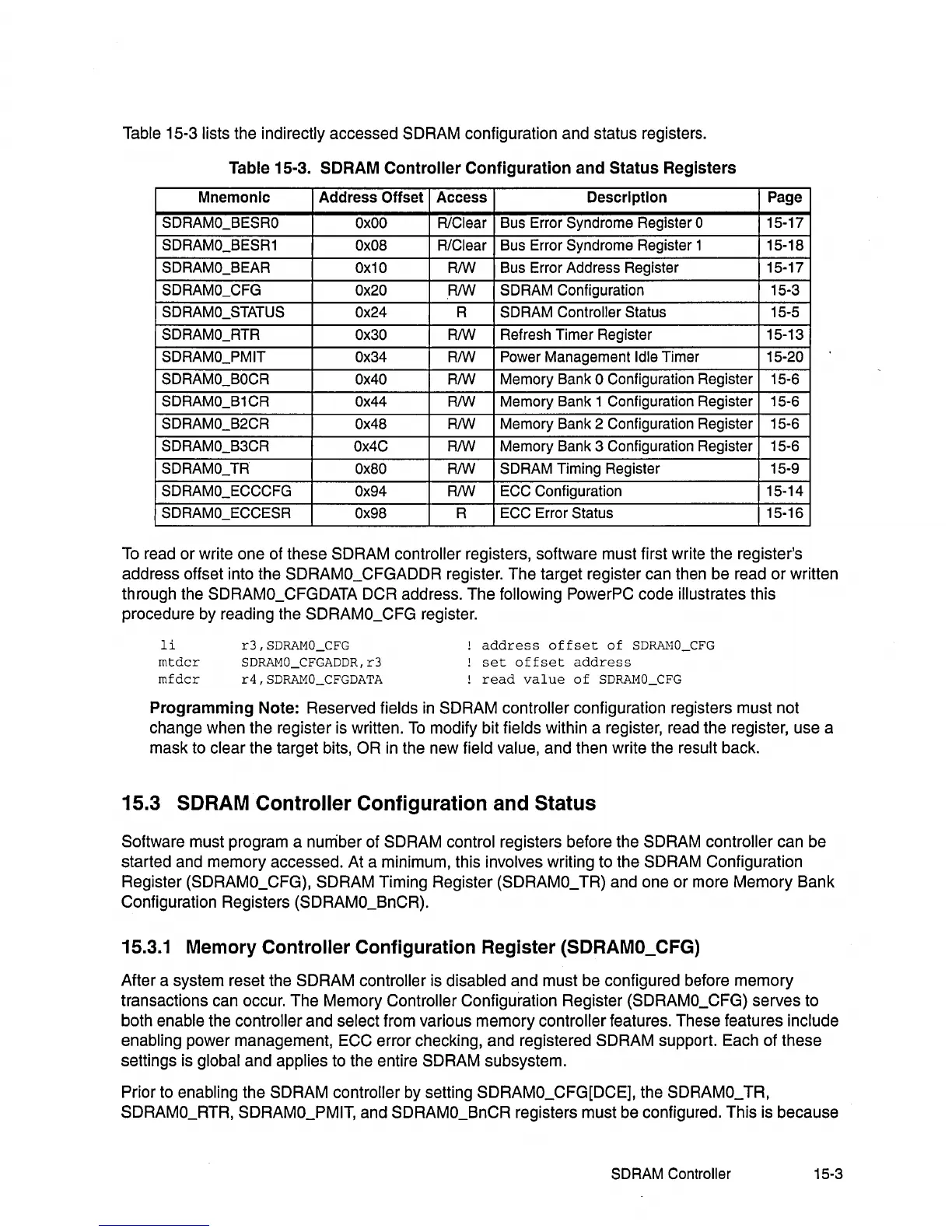
Table 15-3 lists the indirectly accessed SDRAM configuration and status registers.
Table 15·3. SCRAM
Controller
Configuration
and
Status
Registers
Mnemonic Address Offset Access Description
Page
SDRAMO_BESRO
OxOO
RlClear
Bus
Error Syndrome Register 0
15-17
SDRAMO_BESR1
Ox08
R/Clear
Bus
Error Syndrome Register 1 15-18
SDRAMO_BEAR
Ox10
RNI
Bus
Error Address Register 15-17
SDRAMO_CFG
Ox20
ANI
SDRAM
Configuration 15-3
SDRAMO_STATUS
Ox24
R
SDRAM
Controller Status
15-5
SDRAMO_RTR
Ox30
RNI
Refresh Timer Register
15-13
SDRAMO_PMIT
Ox34
ANI
Power
Management Idle Timer 15-20
SDRAMO_BOCR
Ox40
RNI
Memory Bank 0 Configuration Register 15-6
SDRAMO_B1
CR
Ox44
ANI
Memory Bank 1 Configuration Register 15-6
SDRAMO_B2CR
Ox48
RNI
Memory Bank 2 Configuration Register
15-6
SDRAMO_B3CR
Ox4C
RNI
Memory Bank 3 Configuration Register
15-6
SDRAMO_TH
Ox80
RNI
SDRAM
Timing Register
15-9
SDRAMO_ECCCFG
Ox94
RNI
ECC
Configuration 15-14
SDRAMO_ECCESR
Ox98
R
ECC
Error Status 15-16
To
read or write one of these SDRAM controller registers, software must first write the register's
address offset into the SDRAMO_CFGADDR register. The target register can then be read
or
written
through the SDRAMO_CFGDATA DCR address. The
following PowerPC code illustrates this
procedure by reading the
SDRAMO_CFG register.
li
mtdcr
mfdcr
r3,SDRAMO_CFG
SDRAMO_CFGADDR,r3
r4,SDRAMO_CFGDATA
address
offset
of
SDRAHO_CFG
!
set
offset
address
!
read
value
of
SDRAMO_CFG
Programming
Note: Reserved fields
in
SDRAM controller configuration registers must not
change when the register is written.
To
modify bit fields within a register, read the register, use a
mask to clear the target bits,
OR
in
the new field value, and then write the result back.
15.3 SDRAM Controller Configuration and Status
Software must program a nuniber of SDRAM control registers before the SDRAM controller can be
started and memory accessed. At a minimum, this
involves writing to the SDRAM Configuration
Register (SDRAMO_CFG), SDRAM Timing Register (SDRAMO_ TR) and one or more Memory Bank
Configuration Registers (SDRAMO_BnCR).
15.3.1
Memory Controller Configuration Register (SDRAMO_CFG)
After a system reset the SDRAM controller is disabled and must be configured before memory
transactions can occur. The Memory
Controller Configuration Register (SDRAMO_CFG) serves to
both
enable the controller and select from various memory controller features. These features include
enabling
power management, ECC error checking, and registered SDRAM support. Each of these
settings is
global and applies to the entire SDRAM subsystem.
Prior to
enabling the SDRAM controller
by
setting SDRAMO_CFG[DCE], the SDRAMO_ TR,
SDRAMO_RTR,
SDRAMO_PMIT, and SDRAMO_BnCR registers must be configured. This is because
SDRAM
Controller
15-3

 Loading...


