once SDRAMO_CFG[DCE]=1 writing any of the listed
SDRAM
registers does not actually update the
target register. Write access to
SDRAMO_CFG is independent of SDRAMO_CFG[DCE]. However,
software must ensure that the
SDRAM
controller is idle when updating SDRAMO_CFG[3:1 0]. This
guarantees that the register update does not affect any in-progress
SDRAM operations.
Before software enables the
SDRAM
controller by setting SDRAMO_CFG[DCE] it must ensure that
the
SDRAM power-on delay has been satisfied. For example, the IBM 16MB SDRAM requires a
100J.ls
pause; the
64MB
SDRAM
requires a 200llS pause.
Once
enabled, the SDRAM controller
automatically performs the following initialization procedure:
1. Issues the precharge command to
all banks.
2. Waits SDRAMO_ TR[PTA] cycles.
3. Performs eight CAS before RAS refresh cycles, each separated by SDRAMO_ TR[RFTA] clock
cycles)
4. Issues the mode register write command to each bank.
5. Perform eight
CAS
before RAS refresh cycles (each separated by SDRAMO_ TR[RFTA] clock
cycles).
6. Waits SDRAMO_ TR[RFTA] clock cycles.
The
SDRAM is then available for read and write access.
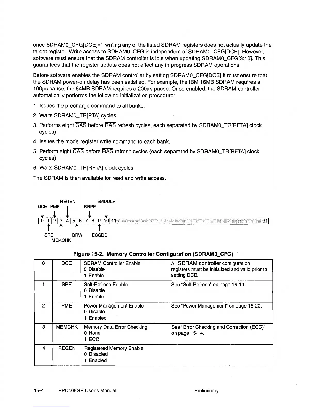
Figure 15-2. Memory Controller Configuration (SDRAMO_CFG)
0
DCE
SDRAM
Controller Enable
All
SDRAM
controller configuration
311
o Disable registers must
be
initialized and valid prior
to
1 Enable
setting
DCE.
1
SRE
Self-Refresh Enable
See
"Self-Refresh"
on
page
15-19.
o Disable
1 Enable
2
PME
Power
Management Enable
See
"Power Management"
on
page 15-20.
o Disable
1 Enabled
3 MEMCHK Memory
Data
Error Checking
See
"Error Checking
and
Correction (ECC)"
o None
on
page 15-14.
1
ECC
4
REGEN
Registered Memory
Enable
o Disabled
1 Enabled
15-4
PPC405GP User's Manual Preliminary

 Loading...


