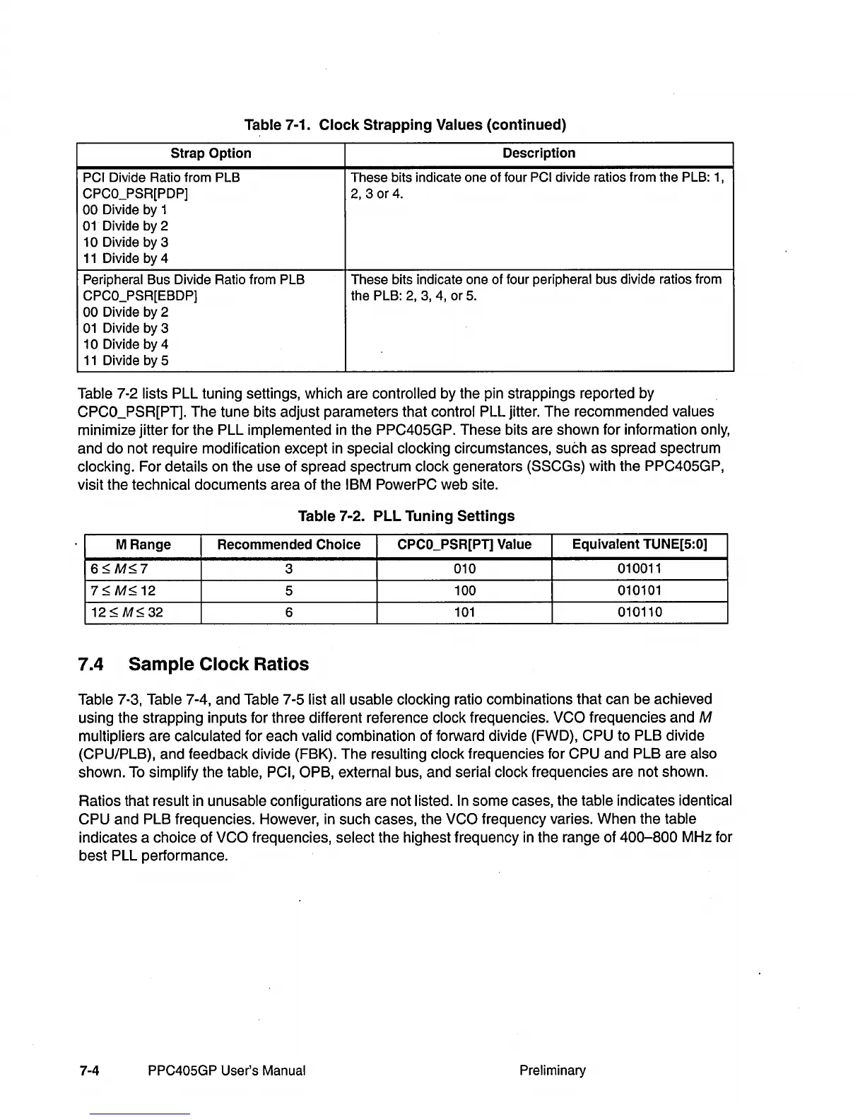
Table 7-1. Clock Strapping Values (continued)
Strap
Option
Description
PCI Divide Ratio from PLB
These bits indicate one of four
PCI divide ratios from the PLB:
1,
CPCO_PSR[PDP]
2,3
or
4.
00 Divide by 1
01
Divide by 2
10 Divide by 3
11
Divide by 4
Peripheral Bus Divide Ratio from PLB
These bits indicate one of four peripheral bus divide ratios from
CPCO_PSR[EBDP] the PLB:
2,
3,
4, or
5.
00 Divide by 2
01
Divide by 3
10 Divide by 4
11
Divide by 5
Table 7-2 lists PLL tuning settings, which are controlled by the pin strappings reported by
CPCO_PSR[PT]. The tune bits adjust parameters that control PLL jitter. The recommended values
minimize jitter for the PLL implemented
in
the PPC405GP. These bits are shown for information only,
and
do
not require modification except
in
special clocking circumstances, such as spread spectrum
clocking. For details on the use of spread spectrum clock generators
(SSCGs) with the PPC405GP,
visit the technical documents area of the
IBM PowerPC web site.
Table 7-2. PLL Tuning Settings
M
Range
Recommended
Choice
CPCO_PSR[PT] Value
Equivalent
TUNE[5:0]
6":;'M":;'7
3
010
010011
7":;'
M":;'
12
5
100
010101
12":;'
M":;'
32
6
101
010110
7.4 Sample
Clock
Ratios
Table 7-3, Table 7-4, and Table 7-5 list all usable clocking ratio combinations that can be achieved
using the strapping inputs for three different reference clock frequencies.
VCO frequencies and M
multipliers are calculated for each valid combination of forward divide (FWD), CPU to PLB divide
(CPU/PLB), and feedback divide (FBK). The resulting clock frequencies for CPU and PLB are also
shown.
To
simplify the table, PCI, OPB, external bus, and serial clock frequencies are not shown.
Ratios that result in unusable configurations are not listed.
In some cases, the table indicates identical
CPU and PLB frequencies. However, in such cases, the
VCO frequency varies. When the table
indicates a choice of
VCO frequencies, select the highest frequency
in
the range of
400-800
MHz for
best PLL performance.
7-4 PPC405GP User's Manual Preliminary