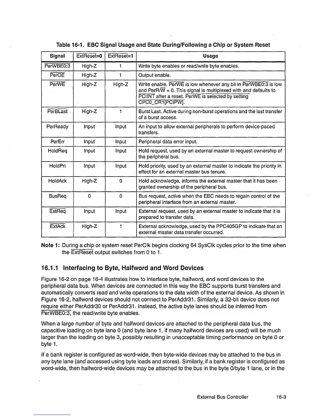
Table 16·1. EBC
Signal
Usage
and
State
During/Following
a
Chip
or
System
Reset
Signal
ExtReset=O ExtReset=1
Usage
PerWBEO:3 High-Z 1 Write byte enables or read/write byte enables.
PerOE
High-Z
1 Output enable.
PerWE
High-Z High-Z Write enable. PerWE is low whenever any bit
in
PerWBEO:3 is low
and
PerRIW =
O.
This signal is multiplexed with and defaults to
PCIINT after a reset. PerWE is selected by setting
CPCO_CR1 [PCIPW].
PerBLast High-Z
1 Burst Last. Active during non-burst operations and the last transfer
of a burst access.
PerReady
Input Input
An
input to allow external peripherals to perform device-paced
transfers.
PerErr
Input
Input Peripheral data error input.
HoldReq
Input Input Hold request, used by an external master to request ownership of
the peripheral bus.
HoldPri
Input Input Hold priority, used by an external master to indicate the priority
in
effect for an external master bus tenure.
HoldAck
High-Z 0 Hold acknowledge, informs the external master that it has been
granted ownership of the peripheral bus.
BusReq
0 0
Bus request, active when the EBC needs to regain control of the
peripheral interface from an external master.
ExtReq
Input Input
External request, used by an external master to indicate that it is
prepared to transfer data.
ExtAck
High-Z
1 External acknowledge, used
by
the PPC405GP to indicate that an
external master data transfer occurred.
Note
1: During a chip or system reset PerClk begins clocking 64 SysClk cycles prior to the time when
the ExtReset output switches from a to 1 .
16.1.1 Interfacing
to
Byte, Halfword and Word Devices
Figure 16-2 on page 16-4 illustrates how to interface byte, halfword, and word devices to the
peripheral data bus. When devices are connected in this way the
ESC supports burst transfers and
automatically converts read and write operations to the data width of the external device. As shown
in
Figure 16-2, halfword devices should not connect to PerAddr31. Similarly, a 32-bit device does not
require either
PerAddr3a or PerAddr31. Instead, the active byte lanes should be inferred from
PerWSEa:3, the read/write byte enables.
When a large number of byte and halfword devices are attached to the peripheral data bus, the
capacitive loading on byte lane a (and byte lane
1,
if many halfword devices are used) will be much
larger than the loading on byte
3,
possibly resulting
in
unacceptable timing performance on byte a or
byte
1.
If a bank register is configured as word-wide, then byte-wide devices may be attached to the bus
in
any byte lane (and accessed using byte loads and stores). Similarly, if a bank register is configured as
word-wide, then halfword-wide devices may be attached to the bus
in
the byte a/byte 1 lane, or
in
the
External Bus Controller 16-3