Programming
Note:
PLB master priority assignments, which are application-dependent, must
be considered
carefully to prevent potential lockouts of lower priority masters. For most
applications, assigning a priority of
Ob10
to each master is a useful starting point.
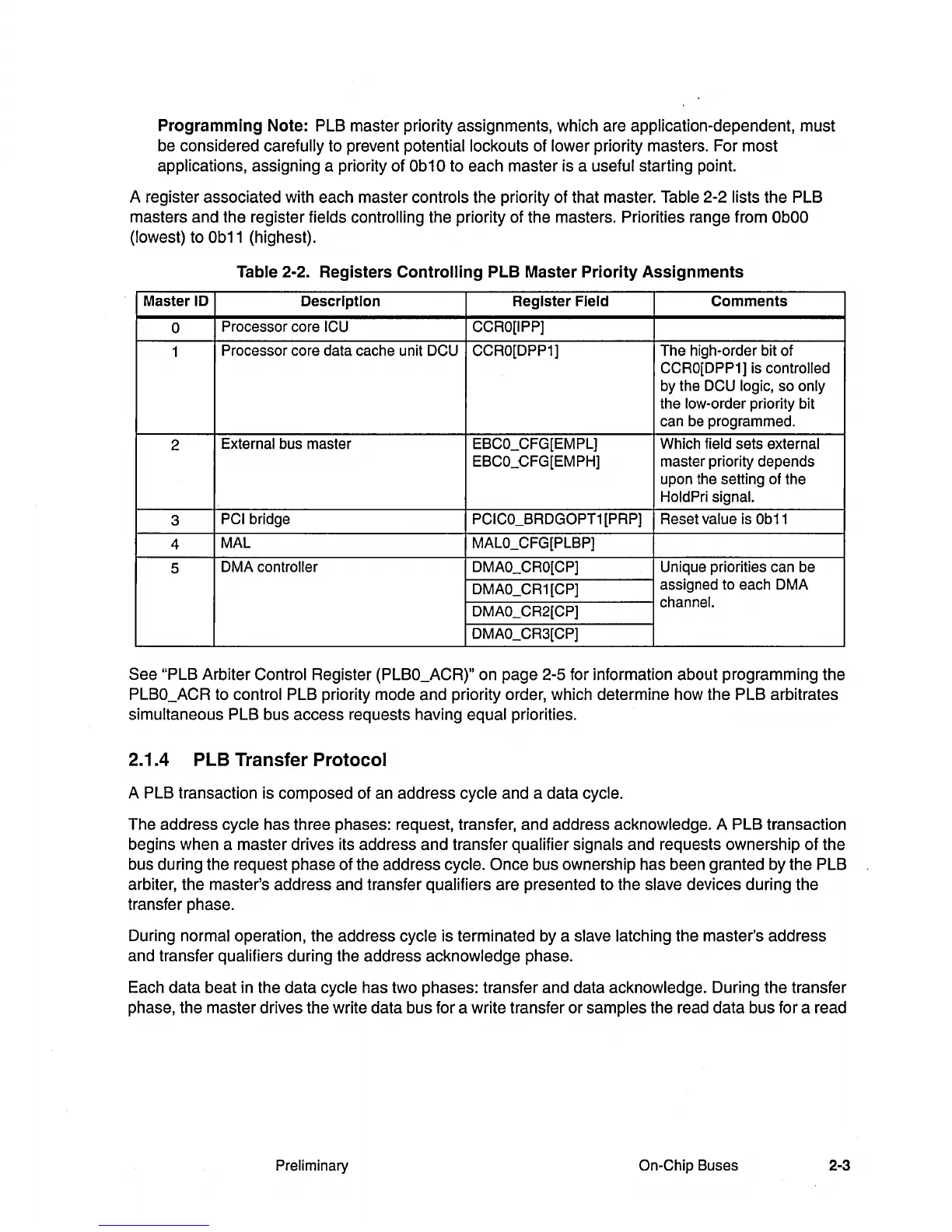
A register associated with each master controls the priority of that master. Table 2-2
lists the PLB
masters and the register fields
controlling the priority of the masters. Priorities range from
ObOO
(lowest) to
Ob11
(highest).
Table 2·2.
Registers
Controlling
PLB
Master
Priority
Assignments
Master
ID
Description
Register
Field
Comments
0
Processor core ICU CCRO[IPP]
1
Processor core data cache unit DCU CCRO[DPP1]
The high-order bit of
CCRO[DPP1] is controlled
by the DCU logic, so only
the low-order priority bit
can be programmed.
2
External bus master EBCO_CFG[EMPL] Which field sets external
EBCO_CFG[EMPH]
master priority depends
upon the setting of the
HoldPri signal.
3
PCI bridge PCICO_BRDGOPT1 [PRP] Reset value is
Ob11
4
MAL MALO_CFG[PLBP]
5
DMA controller DMAO_CRO[CP] Unique priorities can be
DMAO_CR1
[CP]
assigned to each DMA
DMAO_CR2[CP]
channel.
DMAO_CR3[CP]
See "PLB Arbiter Control Register (PLBO_ACR)" on page 2-5 for information about programming the
PLBO_ACR to control PLB priority mode and priority order, which determine how the PLB arbitrates
simultaneous PLB bus access requests having equal priorities.
2.1.4 PLB Transfer Protocol
A PLB transaction is composed of an address cycle and a data cycle.
The address cycle has three phases: request, transfer, and address acknowledge. A PLB transaction
begins when a master drives its address and transfer
qualifier signals and requests ownership of the
bus during the request phase of the address cycle.
Once bus ownership has been granted by the PLB
arbiter, the master's address and transfer
qualifiers are presented to the slave devices during the
transfer phase.
During normal operation, the address cycle is terminated by a slave latching the master's address
and transfer qualifiers during the address acknowledge phase.
Each data beat in the data cycle has two phases: transfer and data acknowledge. During the transfer
phase, the master drives the write data bus for a write transfer or samples the read data bus for a read
Preliminary
On-Chip Buses
2-3