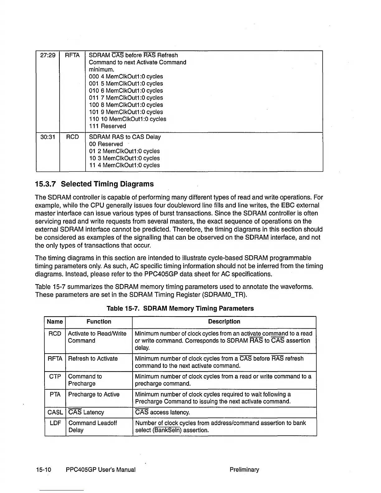
27:29
RFTA
SDRAM CAS before
RAS
Refresh
Command
to
next Activate Command
minimum.
000 4 MemClkOut1
:0
cycles
001
5 MemClkOut1
:0
cycles
010 6 MemClkOut1
:0
cycles
011
7 MemClkOut1
:0
cycles
100 8 MemClkOut1
:0
cycles
101
9 MemClkOut1
:0
cycles
110
10
MemClkOut1:0 cycles
111
Reserved
30:31
RCD
SDRAM
RAS
to
CAS Delay
00 Reserved
01
2 MemClkOut1:0 cycles
10 3 MemClkOut1:0 cycles
11
4 MemClkOut1
:0
cycles
15.3.7 Selected Timing Diagrams
The
SDRArv1
controller is capable
of
performing
many
different
types
of
read
and
write operations. For
example,
while
the
CPU
generally
issues
four doubleword line fills
and
line writes, the
ESC
external
master
interface
can
issue
various
types
of
burst transactions. Since the
SDRAM
controller is often
servicing read
and
write requests from several masters, the exact
sequence
of
operations
on
the
external
SDRAM
interface cannot
be
predicted. Therefore, the timing
diagrams
in this section should
be
considered
as
examples
of
the signalling
that
can
be
observed
on
the
SDRAM
interface,
and
not
the
only
types
of
transactions that occur.
The
timing
diagrams
in this section
are
intended
to
illustrate cycle-based
SDRAM
programmable
timing
parameters
only.
As
such, AC specific timing information should
not
be
inferred from the timing
diagrams.
Instead, please refer to the
PPC405GP
data
sheet
for AC specifications.
Table 15-7
summarizes
the
SDRAM
memory
timing
parameters
used
to
annotate
the waveforms.
These
parameters
are
set
in the
SDRAM
Timing
Register
(SDRAMO_ TR).
Table 15-7. SDRAM Memory Timing Parameters
Name
Function Description
RCD
Activate to ReadlWrite Minimum number of clock cycles from
an
activate command
to
a
read
Command or write command. Corresponds
to
SDRAM
RAS
to
CAS
assertion
delay.
RFTA
Refresh to Activate Minimum number of clock cycles from a CAS before
RAS
refresh
command to the next activate command.
CTP
Command
to
Minimum number of clock cycles from a read or write command
to
a
Precharge
precharge command.
PTA
Precharge to Active Minimum number of clock cycles required
to
wait following a
Precharge Command
to
issuing the next activate command.
CASL
CAS
Latency
CAS
access latency.
LDF Command Leadoff
Number of clock cycles from address/command assertion
to
bank
Delay
select (8ankSeln) assertion.
15-10
PPC405GP User's Manual Preliminary