Chapter 15. SDRAM Controller
The SDRAM controller provides a 32-bit interface to SDRAM memory with optional Error Checking
and Correction (ECC). The memory controller provides
flexible, fully programmable timings for
interfacing to a wide variety of SDRAM devices.
It supports four physical banks of dual-
or
quad-bank
SDRAMs, where each
physical bank is from 4 MB to 256
MBin
size.
In
addition, the SDRAM
controller supports the use of registered SDRAMs.
The controller supports page mode operation with bank
interleaving and maintains up to four open
pages.
To
improve performance, the controller features separate 32-byte read and 128-byte write
buffers. For
applications where data integrity must be guaranteed, optional ECC provides standard
single error correction and double error detection. Designers also have the opportunity to reduce
system power by
placing the SDRAM controller in sleep andlor self-refresh mode.
15.1
Interface Signals
In
many systems the memory controller can directly interface to SDRAM, relieving designers from the
need to buffer
signals
or
add circuitry to phase adjust the SDRAM clock. However, since each
application is different, a detailed timing analysis should always be performed. Please note that all of
the
signals on the SDRAM interface utilize industry standard bit and byte lane numbering. That is,
MemDataO is the
least significant bit and
DQMO
is the enable for the MemData7:0.
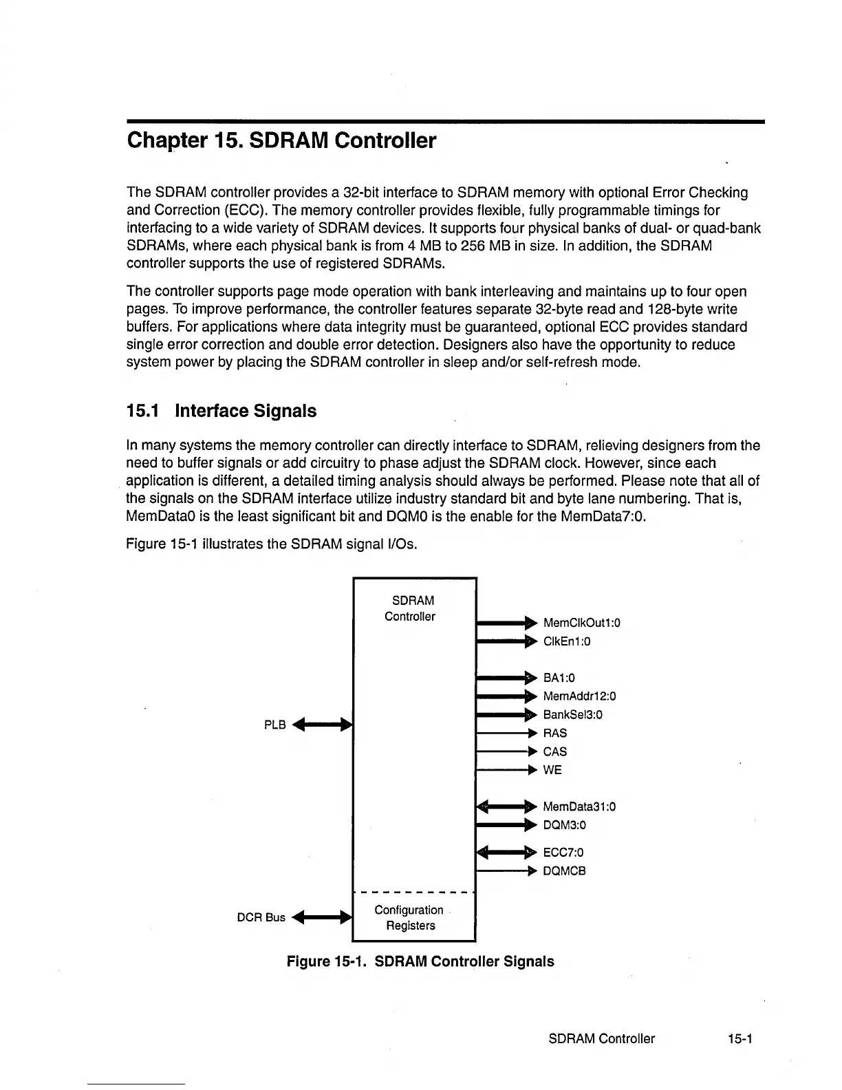
Figure 15-1 illustrates the SDRAM
signal liDs.
SDRAM
Controller
PLB
.....
...
"""
...-
----------
.....
...
Configuration
....
...
Registers
DCR
Bus
..
::
...
..
::
:
...-
..
...
~
..
~
....
..
....
::
....
....
..
....
....
..
~
MemClkOut1
:0
ClkEn1:0
BA1:0
MemAddr12:0
BankSel3:0
RAS
CAS
WE
MemData31
:0
DOM3:0
ECC7:0
DOMCB
Figure 15·1. SDRAM Controller Signals
SDRAM Controller
15-1

 Loading...


