16.2.2 Single Write Transfer
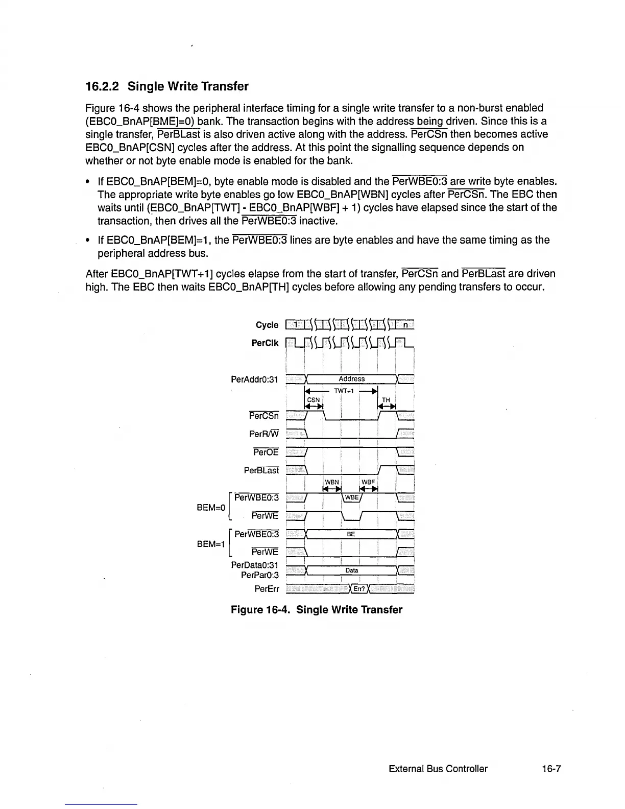
Figure 16-4 shows the peripheral interface timing for a single write transfer to a non-burst enabled
(EBCO_BnAP[BME]=O) bank. The transaction begins with the address being driven. Since this is a
single transfer, PerBLast is
also driven active along with the address. PerCSn then becomes active
EBCO_BnAP[CSN] cycles after the address. At this point the signalling sequence depends on
whether
or
not byte enable mode is enabled for the bank.
• If EBCO_BnAP[BEM]=O, byte enable mode is disabled and the PerWBEO:3 are write byte enables.
The appropriate write byte enables go
low EBCO_BnAP[WBN] cycles after PerCSn. The EBC then
waits until
(~BCO_BnAP[TWT]
- EBCO_BnAP[WBF] + 1) cycles have elapsed since the start of the
transaction, then drives
all the PerWBEO:3 inactive.
• If EBCO_BnAP[BEM]=1, the PerWBEO:3 lines are byte enables and have the same timing as the
peripheral address bus.
After
EBCO_BnAP[TWT + 1] cycles elapse from the start of transfer, PerCSn and PerBLast are driven
high. The
EBC then waits EBCO_BnAP[TH] cycles before allowing any pending transfers to occur.
Cycle o:ntntntntntuL
PerClk
flllW1W1W1Y1Ul;
PerAddrO:31
~
Address C
I~S~I
TWT+l
~
perCsn~
PerR/W ==' C
PerOE
=....J
;C
PerBLast
~
'r--C.
~-,.l-~,
W-BN-'---'-W-B--J
F
!
[
perWBEO:3
d
f+-+I@~
LJ
BEM=O
~--,;
,--_--;.
PerWE:.=1
\-J
L
[
perWBEO:3
-::::J,--.,...--~B;;.:::E_---:-~C
BEM=1
--
:==\'
"
;,.---r
PerWE
~
U
PerDataO:31
----'II,',
,
::,
PerParO:3
--/I
Data
f\--...'.
PerErr
_~~_
......
'&J.,---
__
Figure 16-4. Single Write Transfer
External Bus Controller 16-7