1
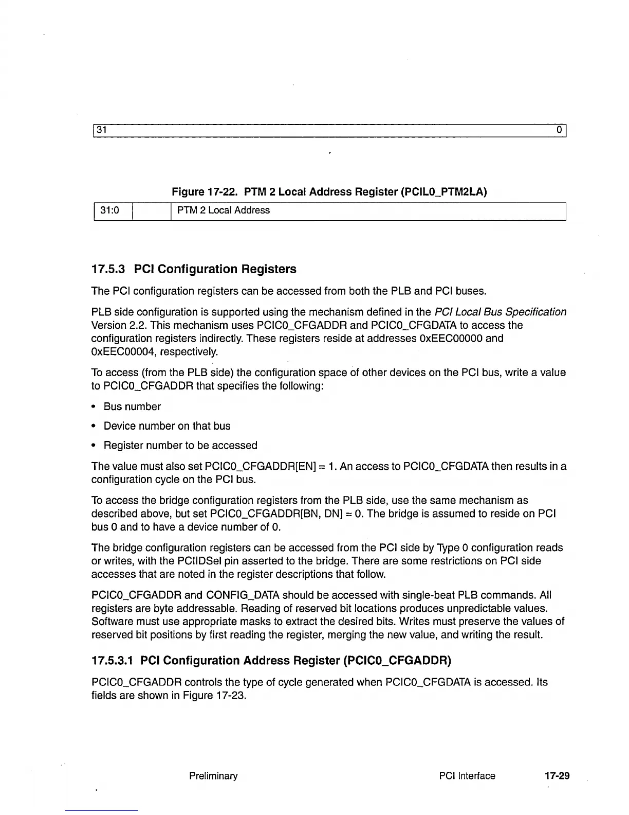
31
01
Figure 17-22.
PTM
2 Local Address Register (PCILO_PTM2LA)
I 31:0 I PTM 2 Local Address
17.5.3 PCI
Configuration
Registers
The PCI configuration registers can be accessed from both the PLB and
PCI
buses.
PLB side configuration is supported using the mechanism defined in the PCI Local Bus Specification
Version 2.2. This mechanism uses PCICO_CFGADDR and PCICO_CFGDATA
to
access the
configuration registers
indirectly. These registers reside at addresses
OxEECOOOOO
and
OxEEC00004, respectively.
To
access (from the PLB side) the configuration space of other devices on the PCI bus, write a value
to PCICO_CFGADDR that specifies the following:
•
Bus number
• Device number on that bus
• Register number to be accessed
The
value must also set PCICO_CFGADDR[EN] =
1.
An access to PCICO_CFGDATA then results
in
a
configuration
cycle on the PCI bus.
To
access the bridge configuration registers from the PLB side, use the same mechanism as
described above, but set
PCICO_CFGADDR[BN, ON] =
o.
The bridge is assumed to reside on PCI
bus 0 and to have a device number of
O.
The bridge configuration registers can be accessed from the PCI side by Type 0 configuration reads
or writes, with the
PCIIDSel pin asserted to the bridge. There are some restrictions on PCI side
accesses that are noted
in
the register descriptions that follow.
PCICO_CFGADDR
and CON FIG_DATA should be accessed with single-beat PLB commands. All
registers are byte addressable. Reading of reserved bit locations produces unpredictable values.
Software must use appropriate masks to extract the desired bits. Writes must preserve the values of
reserved bit positions by first reading the register, merging the new
value, and writing the result.
17.5.3.1
PCI
Configuration Address Register (PCICO_CFGADDR)
PCICO_CFGADDR controls the type of cycle generated when PCICO_CFGDATA is accessed. Its
fields
are shown
in
Figure 17-23.
Preliminary PCI Interface
17-29