12.4
JTAG
Connector
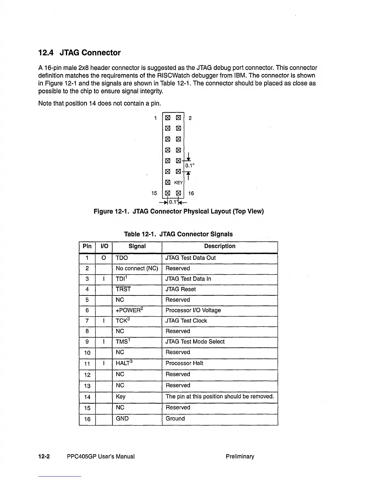
A 16-pin male 2x8 header connector is suggested as the JTAG debug port connector. This connector
definition matches the requirements of the
RISCWatch debugger from
18M.
The connector is shown
in Figure 12-1 and the signals are shown
in
Table 12-1. The connector should be placed as close as
possible to the chip to ensure
signal integrity.
Note that position 14 does not contain a pin.
181
KEY
15
181 181
16
Figure 12-1.
JTAG
Connector Physical Layout (Top View)
Table 12-1.
JTAG
Connector Signals
Pin
1/0
Signal
Description
1
0
TDO
JTAG Test Data Out
2 No connect (NC) Reserved
3
I
TDI1
JTAG Test Data
In
4
TRST
JTAG Reset
5
NC
Reserved
6
+POWER
2
Processor I/O Voltage
7 I
TCK
3
JTAG Test Clock
8
NC
Reserved
9 I
TMS1
JTAG Test Mode Select
10
NC
Reserved
11
I HALT
3
Processor Halt
12
NC
Reserved
13
NC
Reserved
14
Key
The pin at this position should be removed.
15
NC Reserved
16
GND
Ground
12-2
PPC405GP User's Manual
Preliminary