1 . A 10K ohm pullup resistor should be connected to this signal to reduce chip power consumption.
The
pullup resistor is not required.
2. The +POWER signal, sourced from the target development board, indicates whether the
liD
voltage at which the processor is operating. This signal does not supply power to the RISCWatch
hardware
or
to the processor. The active level on this signal can be +5V
or
+3.3V (note that the
PPC405GP can have either +5V
or
+3.3V
liD,
but the processor itself
mustbe
powered by +3.3V).
A series resistor
(1
K ohm
or
less) should be used to provide short circuit current-limiting protection.
3.
A 10K ohm pullup resistor must be connected to these signals to ensure proper chip operation
when these inputs are not used.
12.4.1
JTAG
Instructions
The JTAG debug port provides the standard extest, idcode, sample/preload, and bypass instructions
and the optional
highz and clamp instructions. Invalid instructions behave as the bypass instruction.
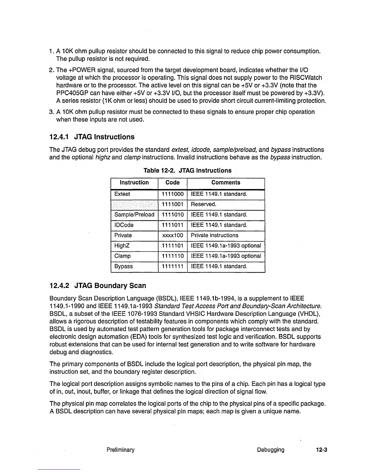
Table 12-2. JTAG
Instructions
Instruction
Code
Comments
Extest 1111000 IEEE 1149.1 standard.
1111001 Reserved.
Sample/Preload 1111010 IEEE 1149.1 standard.
IDCode 1111011 IEEE 1149.1 standard.
Private xxxx100 Private instructions
HighZ 1111101
IEEE 1149.1a-1993 optional
Clamp
1111110 IEEE 1149.1a-1993 optional
Bypass 1111111
IEEE 1149.1 standard.
12.4.2
JTAG
Boundary Scan
Boundary Scan Description Language (BSDL), IEEE 1149.1b-1994, is a supplement to IEEE
1149.1-1990 and IEEE 1149.1 a-1993 Standard Test Access Port
and
Boundary-Scan Architecture.
BSDL, a subset of the IEEE 1076-1993 Standard VHSIC Hardware Description Language (VHDL),
allows a rigorous description of testability features in components which comply with the standard.
BSDL is used by automated test pattern generation tools for package interconnect tests and by
electronic design automation (EDA) tools for synthesized test logic and verification.
BSDL supports
robust extensions that can be used for internal test generation and to write software for hardware
debug and diagnostics.
The primary components of
BSDL include the logical port description, the physical pin map, the
instruction set, and the boundary register description.
The logical port description assigns symbolic names to the pins of a chip. Each pin has a logical type
of
in, out, inout, buffer,
or
linkage that defines the logical direction of signal flow.
The physical pin map correlates the logical ports of the chip to the physical pins of a specific package.
A
BSDL description can have several physical pin maps; each map is given a unique name.
Preliminary
Debugging
12-3

 Loading...


