000
t
*
12113
15
1
16
31
1
IV
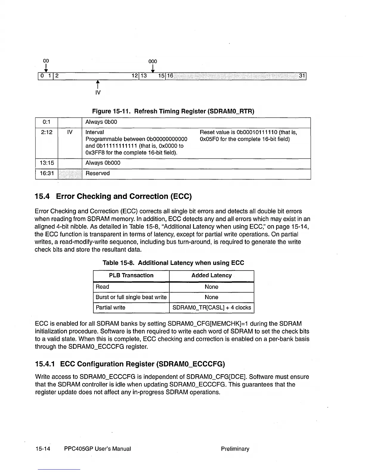
Figure 15·11. Refresh
Timing
Register (SDRAMO_RTR)
0:1
Always
ObOO
2:12
IV
Interval Reset value
is
Ob0001
011111
0 (that
is,
Programmable between
ObOOOOOOOOOOO
Ox05FO
for the complete 16-bit field)
and
Ob11111111111
(that
is,
OxOOOO
to
Ox3FF8
for the complete 16-bit field).
13:15
Always
ObOOO
16:31
Reserved
15.4 Error Checking and Correction (ECC)
Error Checking and Correction (ECC) corrects all single bit errors and detects all double bit errors
when reading from
SDRAM memory. In addition, ECC detects any and all errors which may exist
in
an
aligned 4-bit nibble. As detailed
in
Table 15-8, "Additional Latency when using ECC:' on page 15-14,
the
ECC function is transparent
in
terms of latency, except for partial write operations. On partial
writes, a read-modify-write sequence, including bus turn-around, is required to generate the write
check bits and store the
resultant data.
Table 15·8.
Additional
Latency when
using
ECC
PLB Transaction Added Latency
Read
None
Burst or
full single beat write None
Partial write
SDRAMO_
TR[CASL] + 4 clocks
ECC is enabled for all SDRAM banks by setting SDRAMO_CFG[MEMCHK]=1 during the SDRAM
initialization procedure. Software is then required to write each word of SDRAM to set the check bits
to a
valid state. When this is complete, ECC checking and correction is enabled on a per-bank basis
through the SDRAMO_ECCCFG register.
15.4.1
ECC
Configuration Register (SDRAMO_ECCCFG)
Write access to SDRAMO_ECCCFG is independent of SDRAMO_CFG[DCE]. Software must ensure
that the
SDRAM controller is idle when updating SDRAMO_ECCCFG. This guarantees that the
register update does not affect any in-progress
SDRAM operations.
15-14
PPC405GP User's Manual Preliminary