0142530-000 AB KLA-Tencor Confidential 10-5
3/13/09
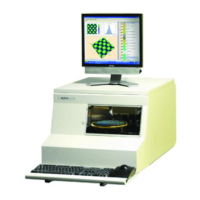
KLA-Tencor P-16+ / P-6 User’s Guide 3D Stress (optional Feature, P-16+ only) -
The 3D Stress Recipe Editor window is similar in content to the 2D Stress Recipe
Editor window, though the layout is different. Definitions of the fields in the 3D
Stress Recipe Editor window are listed below in Table 10.2.
Under the Alignment section, wafer attributes can be selected. See Table 10.3. These
include the wafer notch or flat and location of the notch or flat. This is used as a
reference when the wafer is loaded and unloaded.
In the Substrate Specification section, the user can choose the type of substrate that is
to be scanned as well as input the wafer thickness. The user may choose from a list of
predefined substrates or create new substrates based on their application. See
Table 10.4.
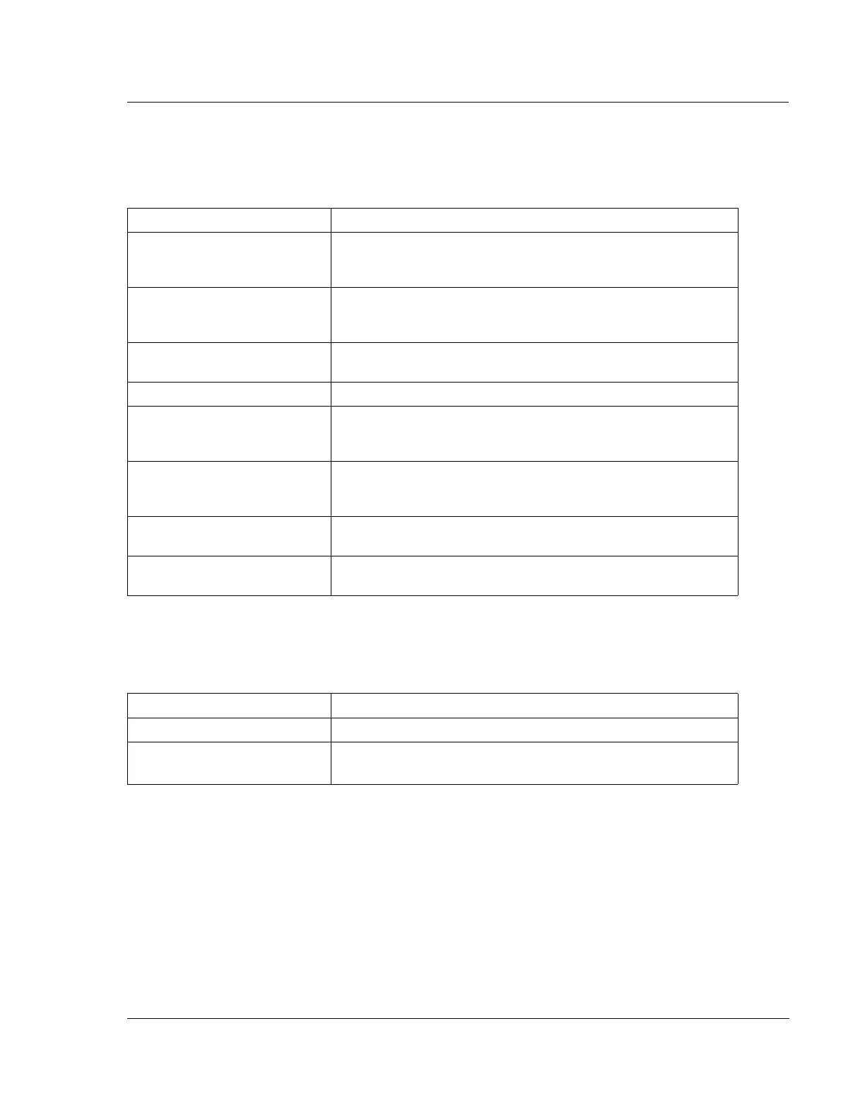
Table 10.2 Field Descriptions in the 3D Stress Recipe Editor Window
Item Description
Wafer Diameter The diameter of the substrate to be scanned. This is a dropdown menu
with entries for the most common wafer sizes. These sizes include 25,
50, 75, 100, 125, 150, and 200mm diameters.
Radial Scan Interval The angular spacing between each successive scan required to build
the 3D image. The dropdown menu values range between 5 and 90
degrees.
Scan Speed Speed at which the stage moves during the scan, The dropdown menu
values range between 1 and 25000 um/s.
Sampling Rate The frequency at which data is captured during the scan.
Auto Level Selecting this box causes the system to perform a stage level before
each 3D profile is performed. By default (unchecked), a stage level is
performed only once after the wafer is loaded.
Scan Length (Read Only) The scan length of the profile is automatically calculated
based on the Wafer Diameter entry. The scan length is 80% of the
inputted Wafer Diameter.
Number of Scans (Read Only) The total number of scans required to build the 3D profile.
This is calculated by dividing 180 by the Radial Scan Interval value.
Total Data Points (Read Only) The total amount of data points collected during the 3D
scans.
Table 10.3 Field Descriptions in the Alignment Section of the Recipe Editor
Item Description
Feature Select feature found on the wafer. Either Notch, Flat, or Square.
Angle
Angle at which the feature is found on the wafer as referenced to
orientation of wafer on the stage.