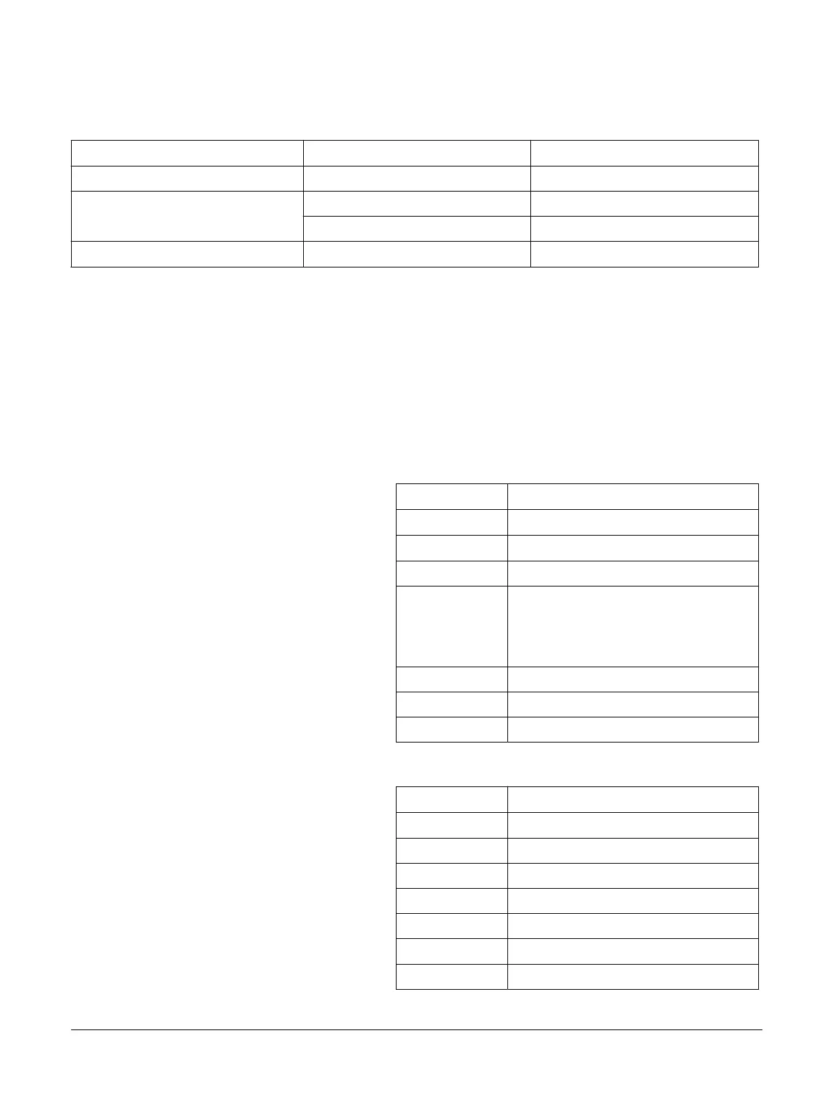
The following table shows the data that is returned from accessing the BPIQ RAM.
Table A6-13 BPIQ cache format
Register Bit field Description
Instruction Register 0 [63:0] Data [63:0]
Instruction Register 1 [63:32] 0
[31:0] Data [95:64]
Instruction Register 2 [63:0] 0
A6.6.2 Encoding for L1 data cache tag, L1 data cache data, and L1 TLB data
The core data cache consists of a 4-way set-associative structure.
The encoding, which is set in Rd in the appropriate MCR instruction, used to locate the required cache data
entry for tag, data, and TLB memory is shown in the following tables. It is similar for both the tag RAM,
data RAM, and TLB access. Data RAM access includes an additional field to locate the appropriate
doubleword in the cache line.
Tag RAM encoding includes an additional field to select which one of the two cache channels must be
used to perform any access.
Table A6-14 L1 data cache tag location encoding
Bit fields of Rd Description
[31:24] RAMID = 0x08
[23:20] Reserved
[19:18] Way
[17]
Copy
0 Tag RAM associated with Pipe 0
1 Tag RAM associated with Pipe 1
[16:14] Reserved
[13:6] Index [13:6]
[5:0] Reserved
Table A6-15 L1 data cache data location encoding
Bit fields of Rd Description
[31:24] RAMID = 0x09
[23:20] Reserved
[19:18] Way
[17:16] BankSel
[15:14] Unused
[13:6] Index [13:6]
[5:0] Reserved
A6 Level 1 memory system
A6.6 Direct access to internal memory
100798_0300_00_en Copyright © 2016–2018 Arm Limited or its affiliates. All rights
reserved.
A6-85
Non-Confidential