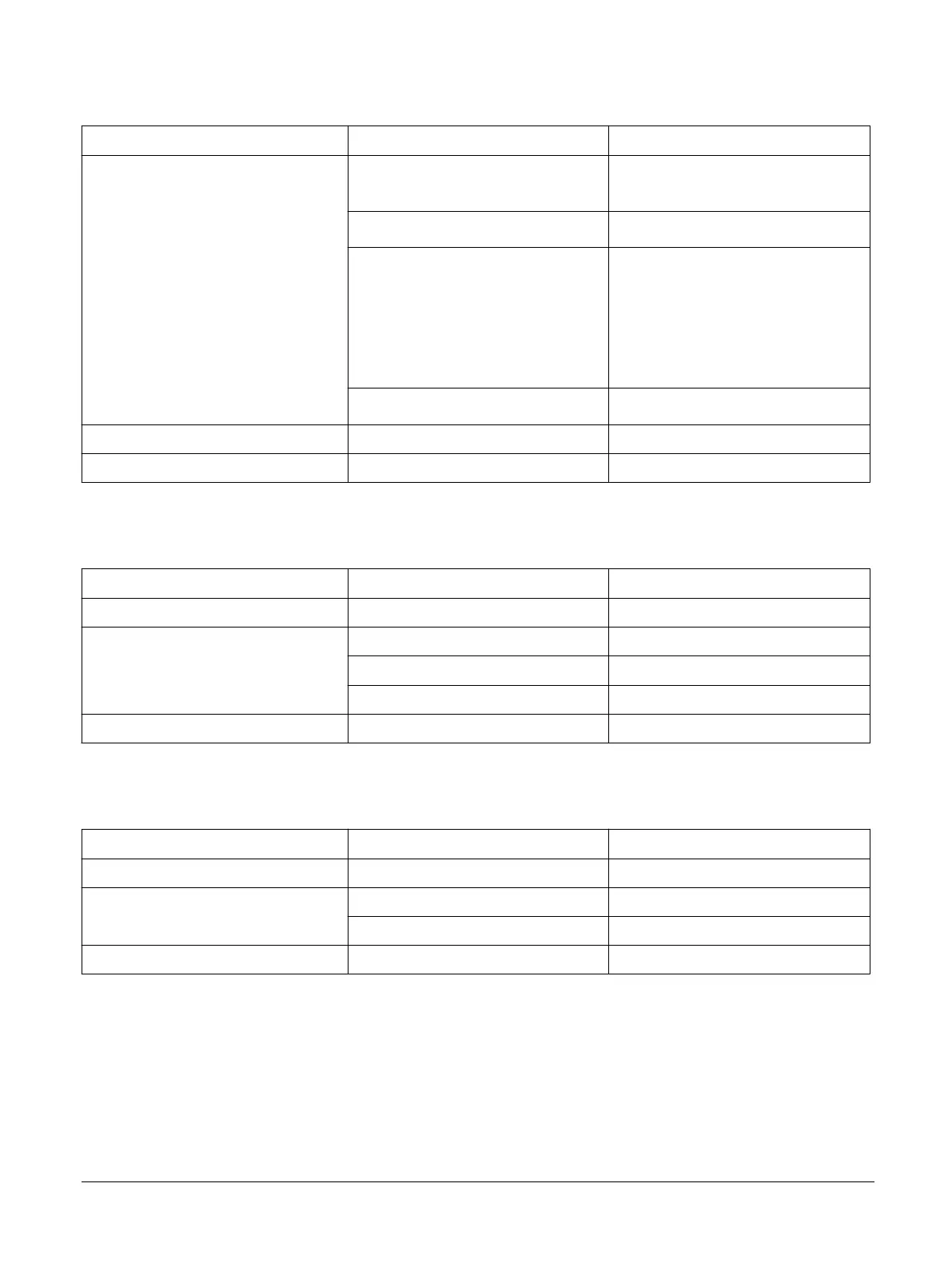
Table A6-8 L1 instruction cache tag format
Register Bit field Description
Instruction Register 0
[31] Non-secure identifier for the physical
address
[30:3] Physical address [39:12]
[2:1]
Instruction state [1:0]
00 Invalid
01 T32
10 A32
11 A64
[0]
Parity
Instruction Register 1 [63:0] 0
Instruction Register 2 [63:0] 0
The following table shows the data that is returned from accessing the L1 instruction data RAM.
Table A6-9 L1 instruction cache data format
Register Bit field Description
Instruction Register 0 [63:0] Data [63:0]
Instruction Register 1 [63:9] 0
[8] Parity
[7:0] Data [71:64]
Instruction Register 2 [63:0] 0
The following table shows the data that is returned from accessing the L1 BTB RAM.
Table A6-10 L1 BTB cache format
Register Bit field Description
Instruction Register 0 [63:0] Data [63:0]
Instruction Register 1 [63:18] 0
[17:0] Data [81:64]
Instruction Register 2 [63:0] 0
The following table shows the data that is returned from accessing the L1 GHB RAM.
A6 Level 1 memory system
A6.6 Direct access to internal memory
100798_0300_00_en Copyright © 2016–2018 Arm Limited or its affiliates. All rights
reserved.
A6-82
Non-Confidential