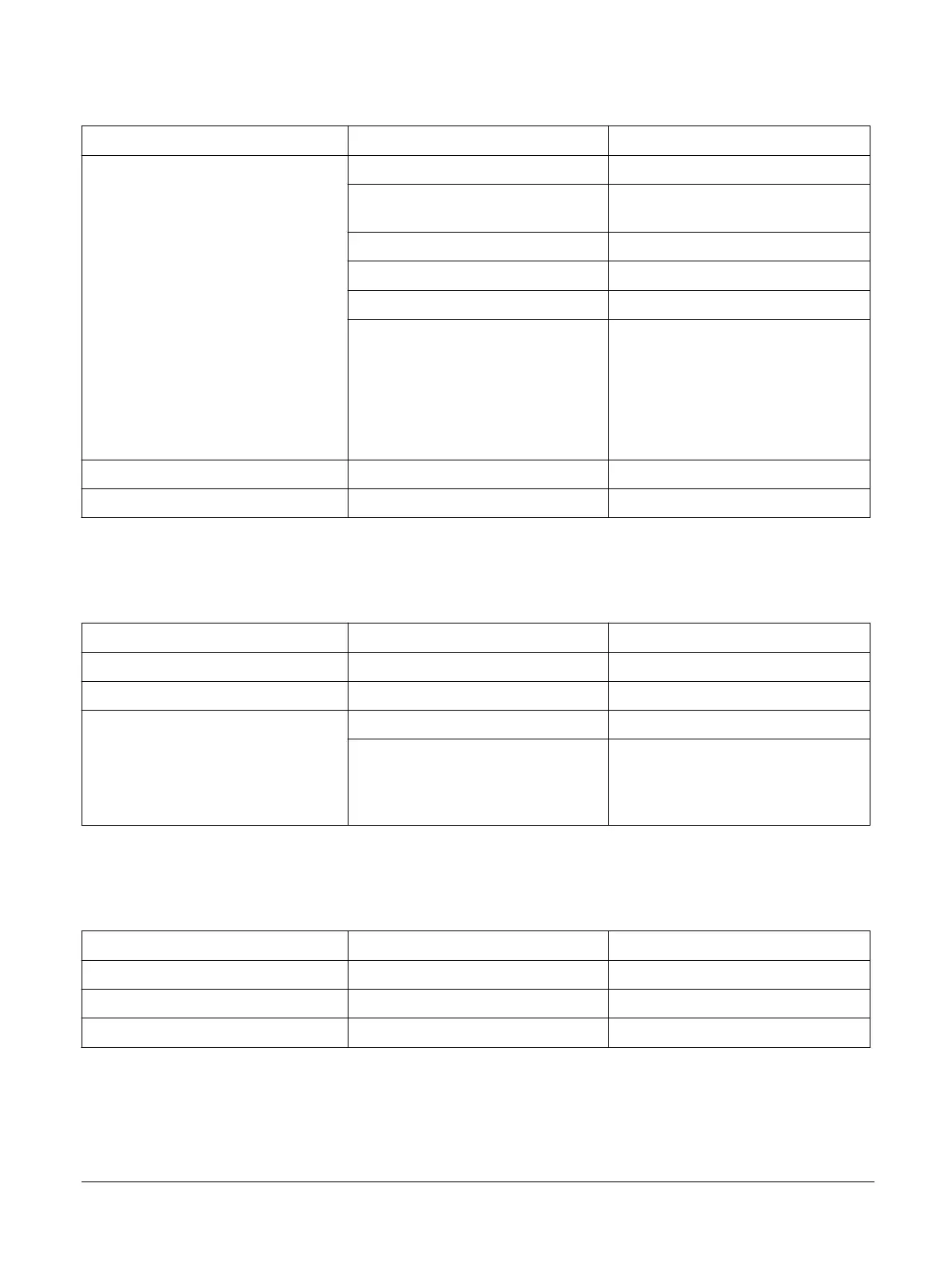
Table A6-18 L1 data cache tag format without ECC
Register Bit field Description
Data Register 0 [63:34] 0
[33] Non-secure identifier for the physical
address
[32:5] Physical address [39:12]
[4:3] Reserved
[2] Transient/WBNA
[1:0]
MESI
00 Invalid
01 Shared
10 Exclusive
11 Modified
Data Register 1 [63:0] 0
Data Register 2 [63:0] 0
The following table shows the data that is returned from accessing the L1 data cache data RAM with
ECC.
Table A6-19 L1 data cache data format with ECC
Register Bit field Description
Data Register 0 [63:0] Word1_data [31:0], Word0_data [31:0]
Data Register 1 [63:0] Word3_data [31:0], Word2_data [31:0]
Data Register 2 [63:32] 0
[31:0] Word3_poison, Word3_ecc [6:0],
Word2_poison, Word2_ecc [6:0],
Word1_poison, Word1_ecc [6:0],
Word0_poison, Word0_ecc [6:0]
The following table shows the data that is returned from accessing the L1 data cache data RAM without
ECC.
Table A6-20 L1 data cache data format without ECC
Register Bit field Description
Data Register 0 [63:0] Word1_data [31:0], Word0_data [31:0]
Data Register 1 [63:0] Word3_data [31:0], Word2_data [31:0]
Data Register 2 [63:0] 0
The following table shows the data that is returned from accessing the L1 data TLB RAM.
A6 Level 1 memory system
A6.6 Direct access to internal memory
100798_0300_00_en Copyright © 2016–2018 Arm Limited or its affiliates. All rights
reserved.
A6-87
Non-Confidential