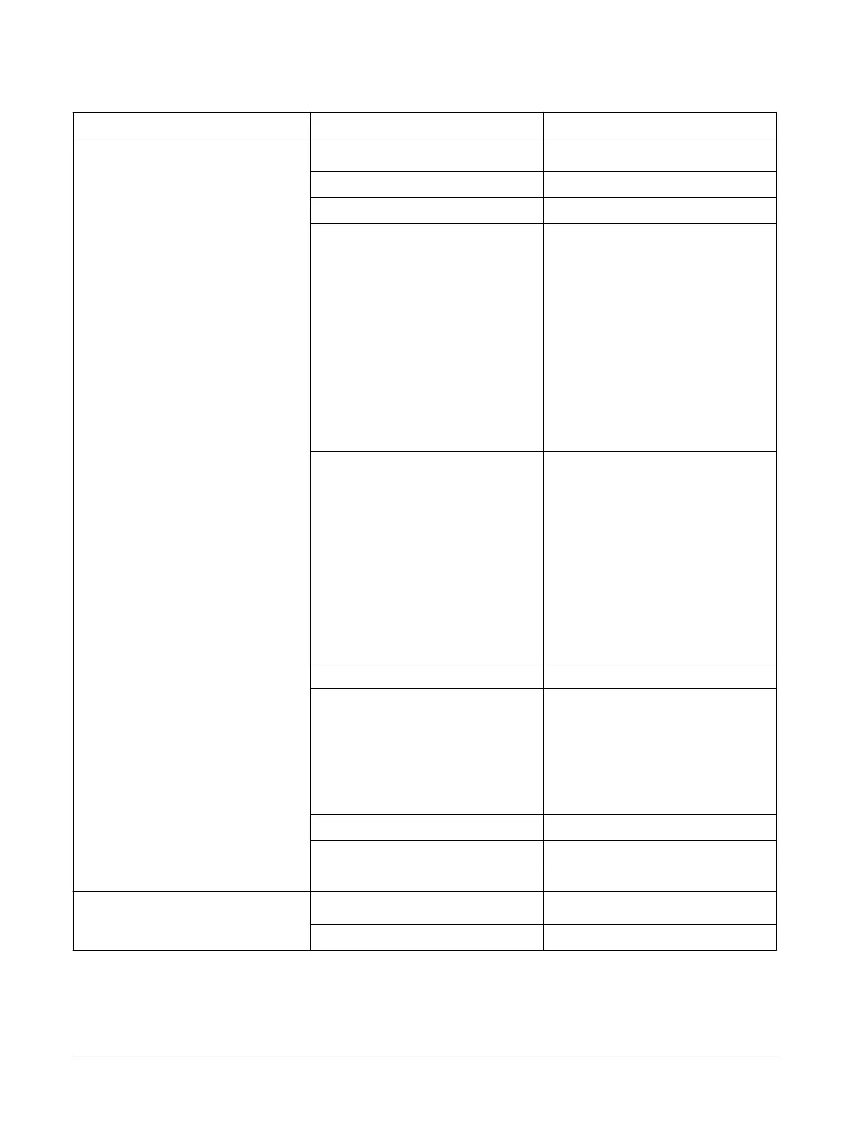
Table A6-21 L1 data TLB cache format
Register Bit field Description
Data Register 0 [63:62]
Virtual address [13:12]
[58] Outer-shared
[57] Inner-shared
[52:50]
Memory attributes:
000 Device nGnRnE
001 Device nGnRE
010 Device nGRE
011 Device GRE
100 Non-cacheable
101 Write-Back No-Allocate
110 Write-Back Transient
111 Write-Back Read-Allocate and
Write-Allocate
[38:36]
Page size:
000 4KB
001 16KB
010 64KB
011 256KB
100 Reserved
101 2MB
110 512MB
111 Reserved
[35] Non-secure
[34:33]
Translation regime:
00 Secure EL1/EL0
01 Secure EL3
10 Non-secure EL1/EL0
11 Non-secure EL2
[32:17] ASID
[16:1] VMID
[0] Valid
Data Register 1 [62:35]
Physical address [39:12]
[34:0] Virtual address[48:14]
A6.6.3 Encoding for the L2 unified cache
The following tables show the encoding required to select a given cache line.
A6 Level 1 memory system
A6.6 Direct access to internal memory
100798_0300_00_en Copyright © 2016–2018 Arm Limited or its affiliates. All rights
reserved.
A6-88
Non-Confidential