Date Code 20151029 SEL-411L Relay
List of Figures
Protection Manual
Figure 1.1 Functional Overview........................................................................................................... P.1.2
Figure 1.2 Two-Terminal Application With Hot Standby Channel...................................................... P.1.9
Figure 1.3 Two-Terminal Application With In-Line Power Transformer and Hot Standby
Channel............................................................................................................................ P.1.9
Figure 1.4 Two-Terminal Application With Hot Standby Channel and Tapped Load
(Load Significantly Less Than Through-Current)........................................................... P.1.9
Figure 1.5 Two-Terminal Application With Voltage Inputs ................................................................. P.1.9
Figure 1.6 Terminal Master/Slave Application With Optional Third Communications Channel ...... P.1.10
Figure 1.7 Four-Terminal Ethernet Application ................................................................................. P.1.10
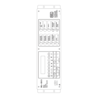
Figure 2.1 Horizontal Front-Panel Template (a); Vertical Front-Panel Template (b)........................... P.2.3
Figure 2.2 Rear 4U Template, Fixed Terminal Block Analog Inputs................................................... P.2.4
Figure 2.3 Standard Control Output Connection.................................................................................. P.2.6
Figure 2.4 Hybrid Control Output Connection..................................................................................... P.2.7
Figure 2.5 High-Speed, High-Current Interrupting Control Output Connection, INTE...................... P.2.8
Figure 2.6 High-Speed, High-Current Interrupting Control Output Connection, INTC...................... P.2.8
Figure 2.7 High-Speed, High-Current Interrupting Control Output Typical Terminals, INTE............ P.2.9
Figure 2.8 Precharging Internal Capacitance of High-Speed, High-Current Interrupting Output
Contacts, INTE................................................................................................................ P.2.9
Figure 2.9 INT2 I/O Interface Board.................................................................................................. P.2.11
Figure 2.10 INTC I/O Interface Board (High Speed)........................................................................... P.2.11
Figure 2.11 INTD I/O Interface Board (Standard)............................................................................... P.2.11
Figure 2.12 INT7 I/O Interface Board.................................................................................................. P.2.11
Figure 2.13 INTE I/O Interface Board ................................................................................................. P.2.11
Figure 2.14 Jumper Location on the Main Board................................................................................. P.2.15
Figure 2.15 Major Jumper and Connector Locations on the Main Board............................................ P.2.16
Figure 2.16 Main Components of the EIA-232 Board, Showing the Location of Serial Port
Jumpers JMP1 and JMP2 .............................................................................................. P.2.17
Figure 2.17 Major Jumper and Connector Locations on the INT2 I/O Board ..................................... P.2.19
Figure 2.18 Major Jumper and Connector Locations on the INTC I/O Board..................................... P.2.20
Figure 2.19 Major Jumper and Connector Locations on the INTE I/O Board..................................... P.2.21
Figure 2.20 Major Jumper and Connector Locations on the INT7 I/O Board ..................................... P.2.22
Figure 2.21 Chassis Dimensions........................................................................................................... P.2.25
Figure 2.22 5U Rear, Main Board With EIA-422 Serial Communications Card in Bay 1, INT2
(200 Slot) and INTE (300 Slot) Interface Boards.......................................................... P.2.26
Figure 2.23 4U Rear, Main Board With 1300 nm IEEE C37.94 Fiber-Optic Serial Communications
Card in Bay 1, EIA-422 Serial Communications Card in Bay 2, 10/100BASE-T
and 100BASE-FX Ethernet Card in Bay 3, INT7 (200 Slot) Interface Board....................... P.2.27
Figure 2.24 5U Rear, Main Board With 850 nm IEEE C37.94 Fiber-Optic Card in Bay 1, EIA-422
Serial Communications Card in Bay 2, 10/100BASE-T and 100BASE-FX in Bay 3,
Standard INTD (200 Slot) and INT 7 (300 Slot) Interface Boards....................................... P.2.27
Figure 2.25 4U Rear, Main Board With EIA-422 Serial Communications Card in Bay 1,
High-Speed INTC (200 Slot) Interface Board............................................................... P.2.28
Figure 2.26 6U Rear, Main Board With EIA-422 Serial Communications Card in Bay 1,
1550 nm Fiber-Optic Communications Card in Bay 2, Four 10/100BASE-T Port
Ethernet Card in Bay 3, High-Speed INTC (200 Slot) Interface Board, INT 7 (300 Slot)
Interface Board, INTE (400 Slot) Interface Board, Connectorized Terminal Blocks for
Current and Voltage Inputs............................................................................................... P.2.28
Figure 2.27 Rear-Panel Symbols.......................................................................................................... P.2.29
Figure 2.28 Screw Terminal Connector Keying ................................................................................... P.2.30
Figure 2.29 Rear-Panel Receptacle Keying.......................................................................................... P.2.31
Figure 2.30 Control Output OUT208 (INT2)....................................................................................... P.2.35