Flash program memory and data EEPROM (FLASH) RM0367
112/1043 RM0367 Rev 7
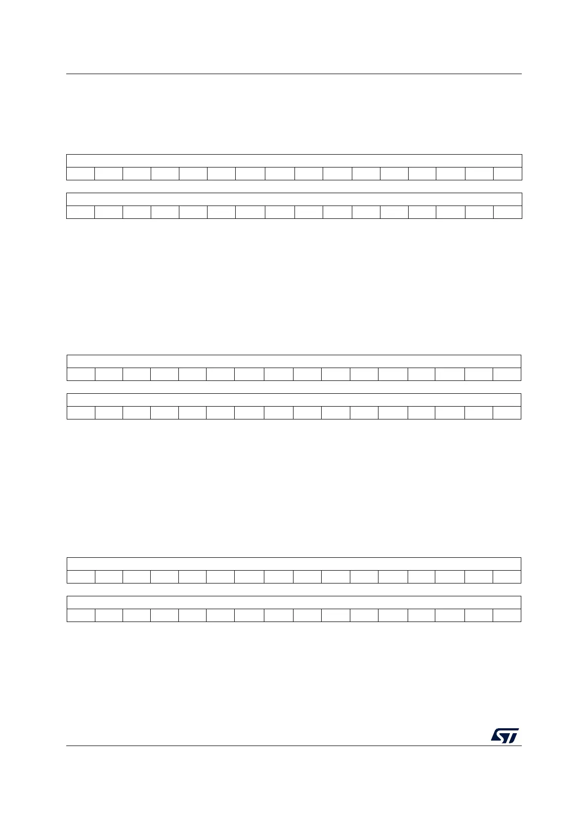
3.7.3 Power-down key register (FLASH_PDKEYR)
Address offset: 0x08
Reset value: 0x0000 0000
3.7.4 PECR unlock key register (FLASH_PEKEYR)
Address offset: 0x0C
Reset value: 0x0000 0000
3.7.5 Program and erase key register (FLASH_PRGKEYR)
Address offset: 0x10
Reset value: 0x0000 0000
31 30 29 28 27 26 25 24 23 22 21 20 19 18 17 16
FLASH_PDKEYR[31:16]
wwwwwww w wwwwwwww
15 14 13 12 11 10 9 8 7 6 5 4 3 2 1 0
FLASH_PDKEYR15:0]
wwwwwww w wwwwwwww
Bits 31:0 This is a write-only register. With a sequence of two write operations (the first one with
0x04152637 and the second one with 0xFAFBFCFD), the write size being that of a word, it is
possible to unlock the RUN_PD bit of the FLASH_ACR register. For more details, refer to
Section 3.6.4: Power-down.
31 30 29 28 27 26 25 24 23 22 21 20 19 18 17 16
FLASH_PEKEYR[31:16]
wwwwww w w www www ww
15 14 13 12 11 10 9 8 7 6 5 4 3 2 1 0
FLASH_PEKEYR15:0]
wwwwww w w www www ww
Bits 31:0 This is a write-only register. With a sequence of two write operations (the first one with
0x89ABCDEF and the second one with 0x02030405), the write size being that of a word, it is
possible to unlock the FLASH_PECR register. For more details, refer to Unlocking the data
EEPROM and the FLASH_PECR register.
31 30 29 28 27 26 25 24 23 22 21 20 19 18 17 16
FLASH_PRGKEYR[31:16]
wwwwww w w www www ww
15 14 13 12 11 10 9 8 7 6 5 4 3 2 1 0
FLASH_PRGKEYR15:0]
wwwwww w w www www ww
Bits 31:0 This is a write-only register. With a sequence of two write operations (the first one with
0x8C9DAEBF and the second one with 0x13141516), the write size being that of a word, it is
possible to unlock the Flash program memory. The sequence can only be executed when
PELOCK is already unlocked. For more details, refer to Unlocking the Flash program memory.