Serial peripheral interface/ inter-IC sound (SPI/I2S) RM0367
886/1043 RM0367 Rev 7
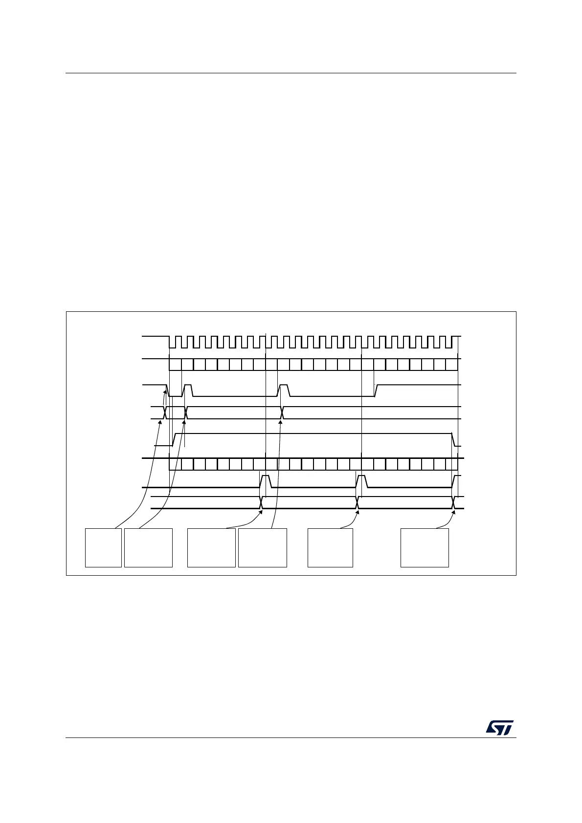
While the master can provide all the transactions in continuous mode (SCK signal is
continuous), it has to respect slave capability to handle data flow and its content at anytime.
When necessary, the master must slow down the communication and provide either a
slower clock or separate frames or data sessions with sufficient delays. Be aware there is no
underflow error signal for slave operating in SPI mode, and that data from the slave are
always transacted and processed by the master even if the slave cannot not prepare them
correctly in time. It is preferable for the slave to use DMA, especially when data frames are
shorter and bus rate is high.
Each sequence must be encased by the NSS pulse in parallel with the multislave system to
select just one of the slaves for communication. In single slave systems, using NSS to
control the slave is not necessary. However, the NSS pulse can be used to synchronize the
slave with the beginning of each data transfer sequence. NSS can be managed either by
software or by hardware (see Section 31.3.4: Multi-master communication).
Refer to Figure 287 and Figure 288 for a description of continuous transfers in master / full-
duplex and slave full-duplex mode.
Figure 287. TXE/RXNE/BSY behavior in master / full-duplex mode (BIDIMODE=0,
RXONLY=0) in the case of continuous transfers
For code example, refer to A.19.3: SPI full duplex communication code example.
MISO/MOSI (in)
Tx buffer
DATA 1 = 0xA1
TXE flag
0xF2
BSY flag
0xF3
software
writes 0xF1
into SPI_DR
software waits
until TXE=1 and
writes 0xF2 into
SPI_DR
software waits
until RXNE=1
and reads 0xA1
from SPI_DR
set by hardware
cleared by software
set by hardware
cleared by software
set by hardware
set by hardware
SCK
DATA 2 = 0xA2
DATA 3 = 0xA3
reset by hardware
Example in Master mode with CPOL=1, CPHA=1
0xF1
RXNE flag
(write SPI_DR)
Rx buffer
set by hardware
MISO/MOSI (out)
DATA1 = 0xF1 DATA2 = 0xF2
DATA3 = 0xF3
(read SPI_DR)
0xA1
0xA2 0xA3
software waits
until TXE=1 and
writes 0xF3 into
SPI_DR
software waits
until RXNE=1
and reads 0xA2
from SPI_ DR
software waits
until RXNE=1
and reads 0xA3
from SPI_DR
b0 b1 b2 b3 b4 b5 b6 b7 b0 b1 b2 b3 b4 b5 b6 b7 b0 b1 b2 b3 b4 b5 b6 b7
b0 b1 b2 b3 b4 b5 b6 b7 b0 b1 b2 b3 b4 b5 b6 b7 b0 b1 b2 b3 b4 b5 b6 b7
cleared by software
ai17343
 Loading...


