Liquid crystal display controller (LCD) RM0367
406/1043 RM0367 Rev 7
17.7 LCD registers
The peripheral registers have to be accessed by words (32-bit).
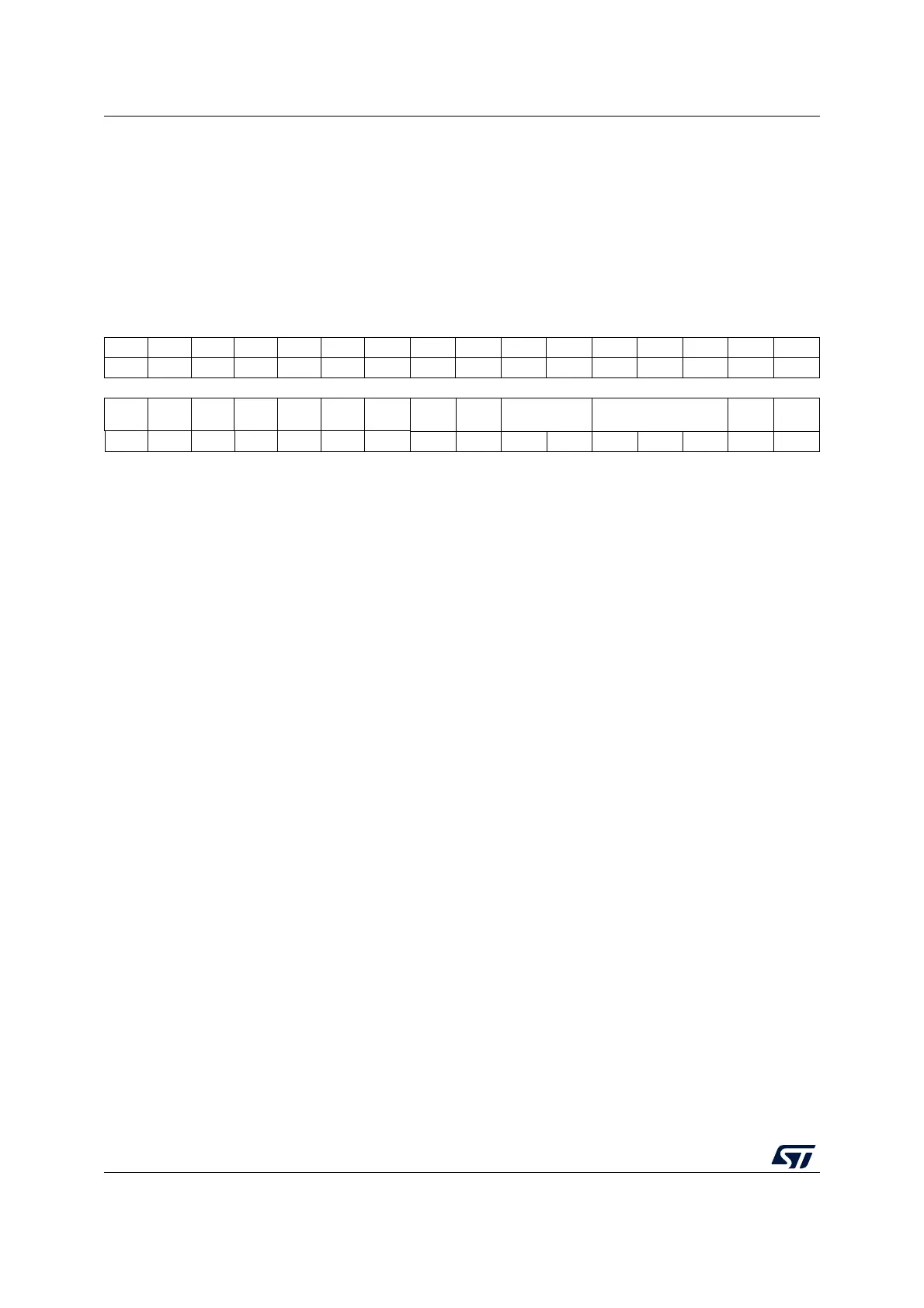
17.7.1 LCD control register (LCD_CR)
Address offset: 0x00
Reset value: 0x0000 0000
31 30 29 28 27 26 25 24 23 22 21 20 19 18 17 16
Res. Res. Res. Res. Res. Res. Res. Res. Res. Res. Res. Res. Res. Res. Res. Res.
1514131211109876543210
Res. Res. Res. Res. Res. Res. Res. Res.
MUX_
SEG
BIAS[1:0] DUTY[2:0] VSEL LCDEN
rw rw rw rw rw rw rw rw
Bits 31:8 Reserved, must be kept at reset value
Bit 7 MUX_SEG: Mux segment enable
This bit is used to enable SEG pin remapping. Four SEG pins can be multiplexed with
SEG[31:28]. See Section 17.4.7.
0: SEG pin multiplexing disabled
1: SEG[31:28] are multiplexed with SEG[43:40]
Bits 6:5 BIAS[1:0]: Bias selector
These bits determine the bias used. Value 11 is forbidden.
00: Bias 1/4
01: Bias 1/2
10: Bias 1/3
11: Reserved
Bits 4:2 DUTY[2:0]: Duty selection
These bits determine the duty cycle. Values 101, 110 and 111 are forbidden.
000: Static duty
001: 1/2 duty
010: 1/3 duty
011: 1/4 duty
100: 1/8 duty
101: Reserved
110: Reserved
111: Reserved
Bit 1 VSEL: Voltage source selection
The VSEL bit determines the voltage source for the LCD.
0: Internal source (voltage step-up converter)
1: External source (VLCD pin)
Bit 0 LCDEN: LCD controller enable
This bit is set by software to enable the LCD Controller/Driver. It is cleared by software to turn
off the LCD at the beginning of the next frame. When the LCD is disabled all COM and SEG
pins are driven to V
SS
. When this bit is set, the ULP bit must be reset in PWR_CR.
0: LCD Controller disabled
1: LCD Controller enabled
 Loading...


