Clock recovery system (CRS) RM0367
232/1043 RM0367 Rev 7
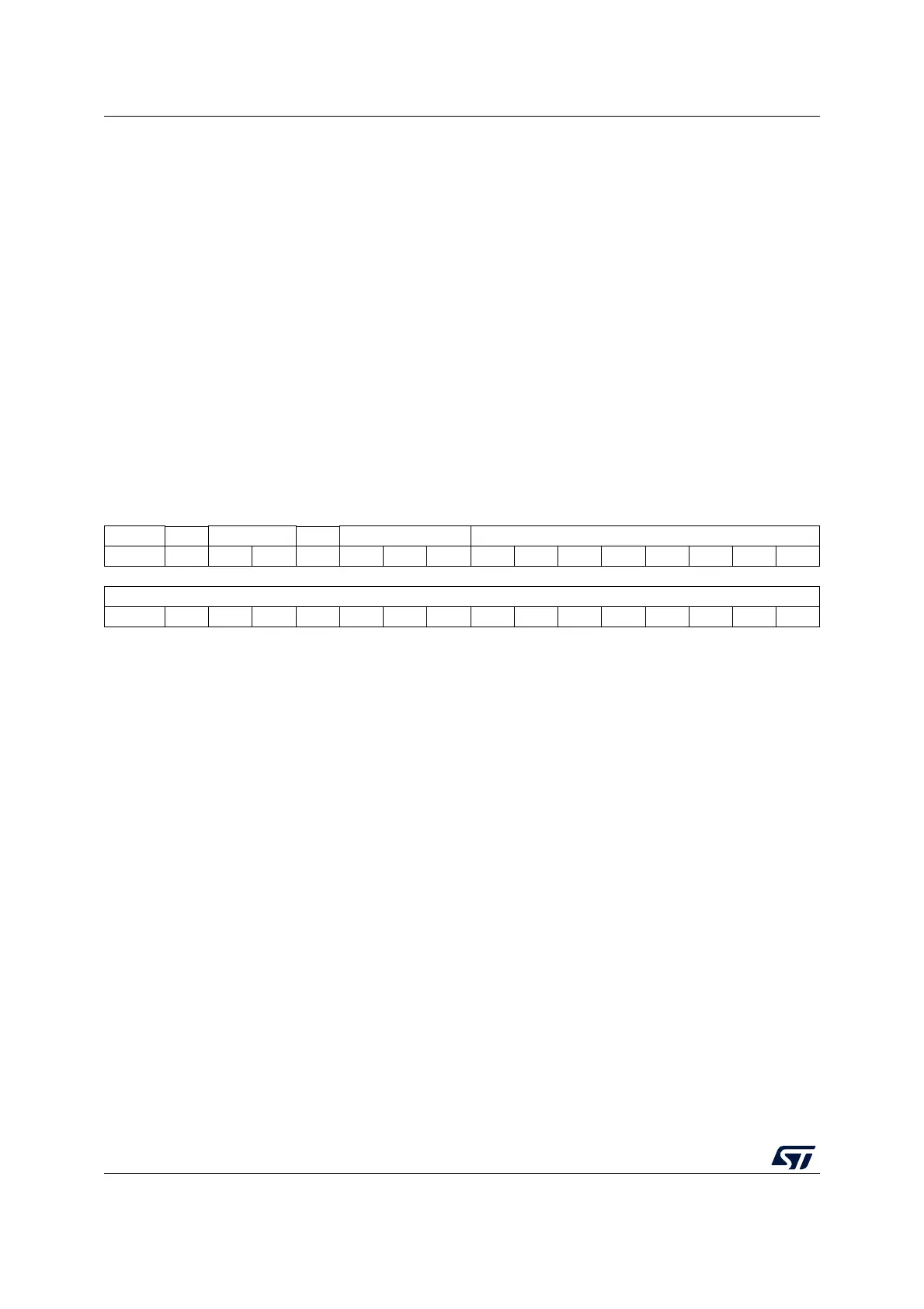
8.7.2 CRS configuration register (CRS_CFGR)
This register can be written only when the frequency error counter is disabled (CEN bit is
cleared in CRS_CR). When the counter is enabled, this register is write-protected.
Address offset: 0x04
Reset value: 0x2022 BB7F
Bit 2 ERRIE: Synchronization or trimming error interrupt enable
0: Synchronization or trimming error (ERRF) interrupt disabled
1: Synchronization or trimming error (ERRF) interrupt enabled
Bit 1 SYNCWARNIE: SYNC warning interrupt enable
0: SYNC warning (SYNCWARNF) interrupt disabled
1: SYNC warning (SYNCWARNF) interrupt enabled
Bit 0 SYNCOKIE: SYNC event OK interrupt enable
0: SYNC event OK (SYNCOKF) interrupt disabled
1: SYNC event OK (SYNCOKF) interrupt enabled
31 30 29 28 27 26 25 24 23 22 21 20 19 18 17 16
SYNCPOL Res. SYNCSRC[1:0] Res. SYNCDIV[2:0] FELIM[7:0]
rw rw rw rw rw rw rw rw rw rw rw rw rw rw
15 14131211109876543210
RELOAD[15:0]
rw rw rw rw rw rw rw rw rw rw rw rw rw rw rw rw
Bit 31 SYNCPOL: SYNC polarity selection
This bit is set and cleared by software to select the input polarity for the SYNC signal source.
0: SYNC active on rising edge (default)
1: SYNC active on falling edge
Bit 30 Reserved, must be kept at reset value.
Bits 29:28 SYNCSRC[1:0]: SYNC signal source selection
These bits are set and cleared by software to select the SYNC signal source.
00: GPIO selected as SYNC signal source
01: LSE selected as SYNC signal source
10: USB SOF selected as SYNC signal source (default).
11: Reserved
Note: When using USB LPM (Link Power Management) and the device is in Sleep mode, the
periodic USB SOF is not generated by the host. No SYNC signal is therefore provided
to the CRS to calibrate the HSI48 oscillator on the run. To guarantee the required clock
precision after waking up from Sleep mode, the LSE or reference clock on the GPIOs
should be used as SYNC signal.
Bit 27 Reserved, must be kept at reset value.