RM0367 Rev 7 309/1043
RM0367 Analog-to-digital converter (ADC)
352
Follow this procedure to disable the ADC:
1. Check that ADSTART = 0 in the ADC_CR register to ensure that no conversion is
ongoing. If required, stop any ongoing conversion by writing 1 to the ADSTP bit in the
ADC_CR register and waiting until this bit is read at 0.
2. Set ADDIS = 1 in the ADC_CR register.
3. If required by the application, wait until ADEN = 0 in the ADC_CR register, indicating
that the ADC is fully disabled (ADDIS is automatically reset once ADEN = 0).
4. Clear the ADRDY bit in ADC_ISR register by programming this bit to 1 (optional).
For code example, refer to A.8.3: ADC disable sequence code example.
Figure 34. Enabling/disabling the ADC
Note: In Auto-off mode (AUTOFF = 1) the power-on/off phases are performed automatically, by
hardware and the ADRDY flag is not set.
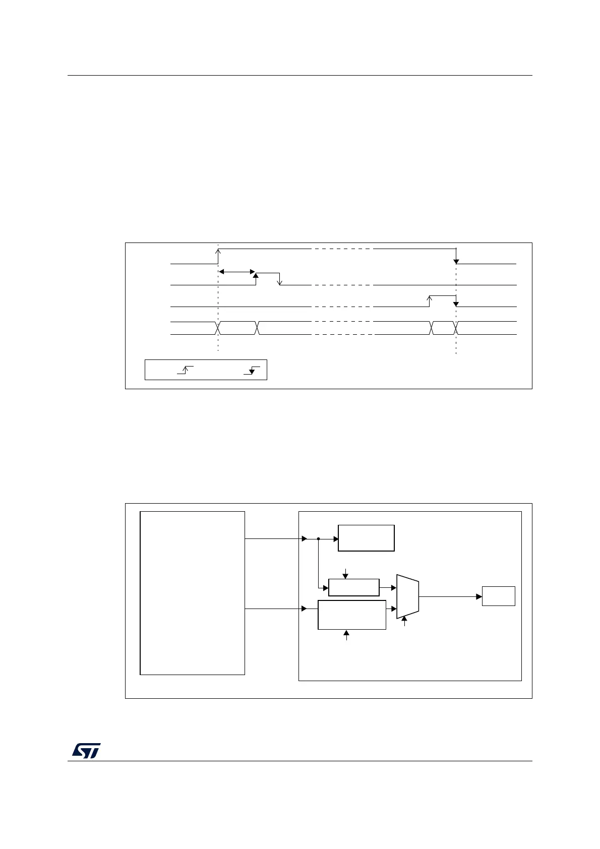
14.3.5 ADC clock (CKMODE, PRESC[3:0], LFMEN)
The ADC has a dual clock-domain architecture, so that the ADC can be fed with a clock
(ADC asynchronous clock) independent from the APB clock (PCLK).
Figure 35. ADC clock scheme
1. Refer to Section Reset and clock control (RCC) for how the PCLK clock and ADC asynchronous clock are
enabled.
MS30264V2
t
STAB
ADEN
DRDY
ADDIS
ADC
OFF Startup RDY CONVERTING CH RDY
OFF
by H/W
by S/W
REQ
-OF
stat
MSv31926V2
ADITF
Analog
ADC
RCC
(Reset & Clock Controller)
PCLK
ADC
asynchronous
clock
APB interface
Analog ADC_CK
/1 or /2 or /4
Others
00
Bits CKMODE[1:0]
of ADC_CFGR2
Bits CKMODE[1:0]
of ADC_CFGR2
/1,2,4,6,8,10,12
16,32,64,128,256
Bits PRESC[3:0]
of ADC_CCR
 Loading...


