General-purpose I/Os (GPIO) RM0367
246/1043 RM0367 Rev 7
9.3.13 Using the HSE or LSE oscillator pins as GPIOs
When the HSE or LSE oscillator is switched OFF (default state after reset), the related
oscillator pins can be used as normal GPIOs.
When the HSE or LSE oscillator is switched ON (by setting the HSEON or LSEON bit in the
RCC_CSR register) the oscillator takes control of its associated pins and the GPIO
configuration of these pins has no effect.
When the oscillator is configured in a user external clock mode, only the OSC_IN or
OSC32_IN pin is reserved for clock input and the OSC_OUT or OSC32_OUT pin can still be
used as normal GPIO.
9.3.14 Using the GPIO pins in the RTC supply domain
The PC13/PC14/PC15 GPIO functionality is lost when the core supply domain is powered
off (when the device enters Standby mode). In this case, if their GPIO configuration is not
bypassed by the RTC configuration, these pins are set in an analog input mode.
For details about I/O control by the RTC, refer to Section 27.4: RTC functional description.
9.4 GPIO registers
For a summary of register bits, register address offsets and reset values, refer to Table 48.
The peripheral registers can be written in word, half word or byte mode.
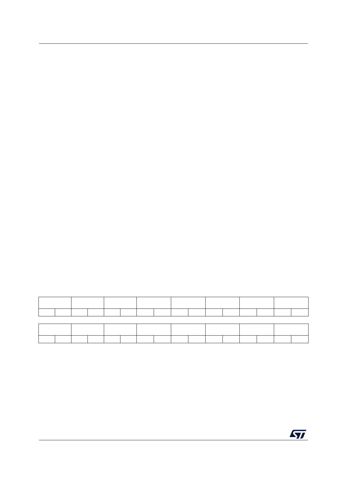
9.4.1 GPIO port mode register (GPIOx_MODER)
(x =A to E and H)
Address offset:0x00
Reset value: 0xEBFF FCFF for port A
Reset value: 0xFFFF FFFF for the other ports
31 30 29 28 27 26 25 24 23 22 21 20 19 18 17 16
MODE15[1:0] MODE14[1:0] MODE13[1:0] MODE12[1:0] MODE11[1:0] MODE10[1:0] MODE9[1:0] MODE8[1:0]
rw rw rw rw rw rw rw rw rw rw rw rw rw rw rw rw
1514131211109876543210
MODE7[1:0] MODE6[1:0] MODE5[1:0] MODE4[1:0] MODE3[1:0] MODE2[1:0] MODE1[1:0] MODE0[1:0]
rw rw rw rw rw rw rw rw rw rw rw rw rw rw rw rw
Bits 31:0 MODE[15:0][1:0]: Port x configuration I/O pin y (y = 15 to 0)
These bits are written by software to configure the I/O mode.
00: Input mode
01: General purpose output mode
10: Alternate function mode
11: Analog mode (reset state)
 Loading...


