RM0367 Rev 7 407/1043
RM0367 Liquid crystal display controller (LCD)
413
Note: The VSEL, MUX_SEG,BIAS, and DUTY bits are write-protected when the LCD is enabled
(ENS bit in LCD_SR to 1).
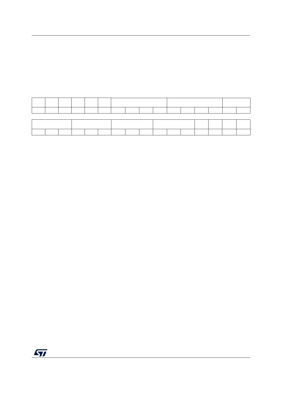
17.7.2 LCD frame control register (LCD_FCR)
Address offset: 0x04
Reset value: 0x0000 0000
31 30 29 28 27 26 25 24 23 22 21 20 19 18 17 16
Res. Res. Res. Res. Res. Res. PS[3:0] DIV[3:0] BLINK[1:0]
rw rw rw rw rw rw rw rw rw rw
15 14 13 12 11 10 9 8 7 6 5 4 3 2 1 0
BLINKF[2:0] CC[2:0] DEAD[2:0] PON[2:0] UDDIE Res. SOFIE HD
rw rw rw rw rw rw rw rw rw rw rw rw rw rw rw
Bits 31:26 Reserved, must be kept at reset value
Bits 25:22 PS[3:0]: PS 16-bit prescaler
These bits are written by software to define the division factor of the PS 16-bit prescaler.
ck_ps = LCDCLK/(2). See
Section 17.4.2.
0000: ck_ps = LCDCLK
0001: ck_ps = LCDCLK/2
0002: ck_ps = LCDCLK/4
...
1111:ck_ps = LCDCLK/32768
Bits 21:18 DIV[3:0]: DIV clock divider
These bits are written by software to define the division factor of the DIV divider. See
Section 17.4.2.
0000: ck_div = ck_ps/16
0001: ck_div = ck_ps/17
0002: ck_div = ck_ps/18
...
1111:ck_div = ck_ps/31
Bits 17:16 BLINK[1:0]: Blink mode selection
00: Blink disabled
01: Blink enabled on SEG[0], COM[0] (1 pixel)
10: Blink enabled on SEG[0], all COMs (up to 8 pixels depending on the programmed duty)
11: Blink enabled on all SEGs and all COMs (all pixels)
Bits 15:13 BLINKF[2:0]: Blink frequency selection
000: f
LCD
/8
001: f
LCD
/16
010: f
LCD
/32
011: f
LCD
/64
100: f
LCD
/128
101: f
LCD
/256
110: f
LCD
/512
111: f
LCD
/1024
 Loading...


