RM0367 Rev 7 389/1043
RM0367 Liquid crystal display controller (LCD)
413
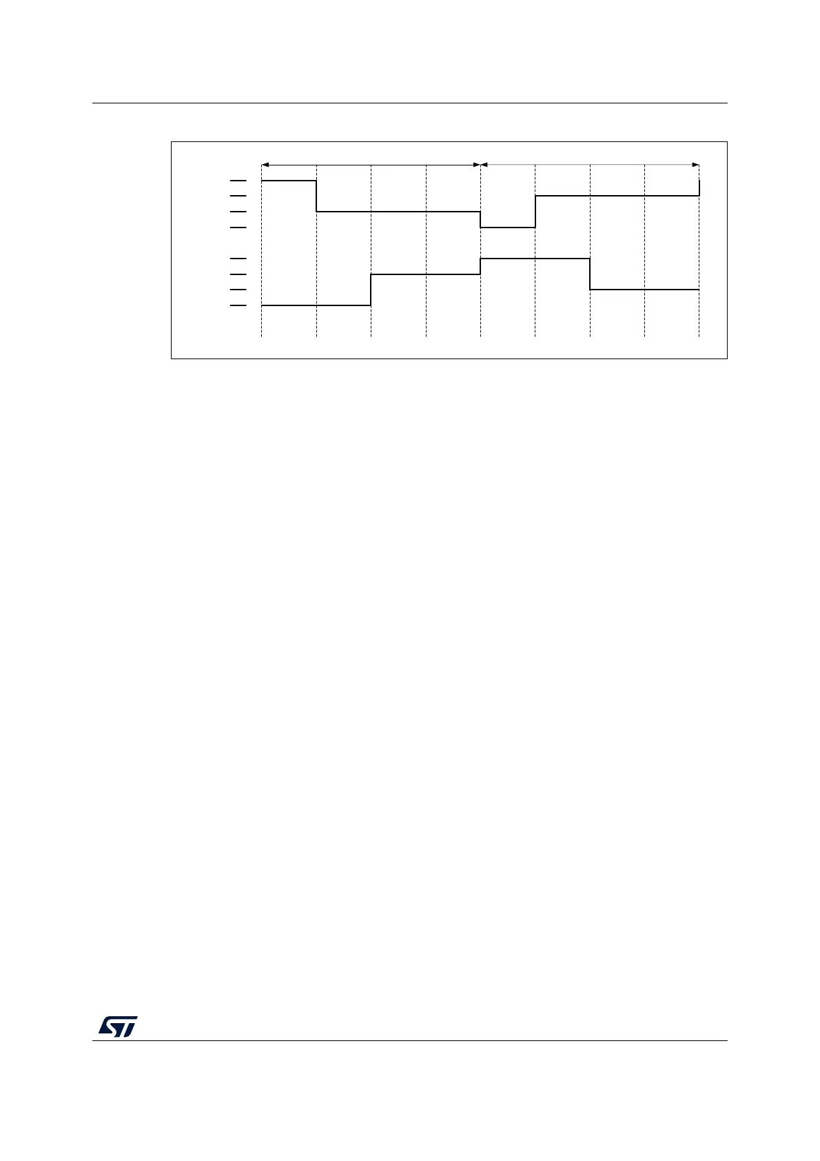
Figure 68. 1/3 bias, 1/4 duty
In case of 1/2 bias (BIAS = 01) the VLCD pin generates an intermediate voltage equal to 1/2
V
LCD
on node b for odd and even frames (see Figure 71).
COM signal duty
Depending on the DUTY[2:0] bits in the LCD_CR register, the COM signals are generated
with static duty (see Figure 70), 1/2 duty (see Figure 71), 1/3 duty (see Figure 72), 1/4 duty
(see Figure 73) or 1/8 duty (see Figure 74).
COM[n] n[0 to 7] is active during phase n in the odd frame, so the COM pin is driven to
V
LCD
.
During phase n of the even frame the COM pin is driven to V
SS
.
In the case of 1/3 or 1/4) bias:
• COM[n] is inactive during phases other than n so the COM pin is driven to 1/3 (1/4)
V
LCD
during odd frames and to 2/3 (3/4) V
LCD
during even frames
In the case of 1/2 bias:
• If COM[n] is inactive during phases other than n, the COM pin is always driven (odd
and even frame) to 1/2 V
LCD
.
When static duty is selected, the segment lines are not multiplexed, which means that each
segment output corresponds to one pixel. In this way only up to 51 pixels can be driven.
COM[0] is always active while COM[7:1] are not used and are driven to V
SS
.
When the LCDEN bit in the LCD_CR register is reset, all common lines are pulled down to
V
SS
and the ENS flag in the LCD_SR register becomes 0. Static duty means that COM[0] is
always active and only two voltage levels are used for the segment and common lines: V
LCD
and V
SS
. A pixel is active if the corresponding SEG line has a voltage opposite to that of the
COM, and inactive when the voltages are equal. In this way the LCD has maximum contrast
(see Figure 69, Figure 70). In the Figure 69 pixel 0 is active while pixel 1 is inactive.
MS33438V1
V
LCD
Odd frame Even frame
Com active
Com inactive Com inactive Com inactive Com active Com inactive Com inactive Com inactive
2/3 V
LCD
1/3 V
LCD
V
SS
V
LCD
2/3 V
LCD
1/3 V
LCD
V
SS
Com active Com active Com inactive Com inactive Com active Com active Com inactive Com inactive
Phase 0 Phase 1 Phase 2 Phase 3 Phase 0 Phase 1 Phase 2 Phase 3
Segment Common
 Loading...


