RM0367 Rev 7 423/1043
RM0367 Touch sensing controller (TSC)
432
18.6 TSC registers
Refer to Section 1.2 on page 52 of the reference manual for a list of abbreviations used in
register descriptions.
The peripheral registers can be accessed by words (32-bit).
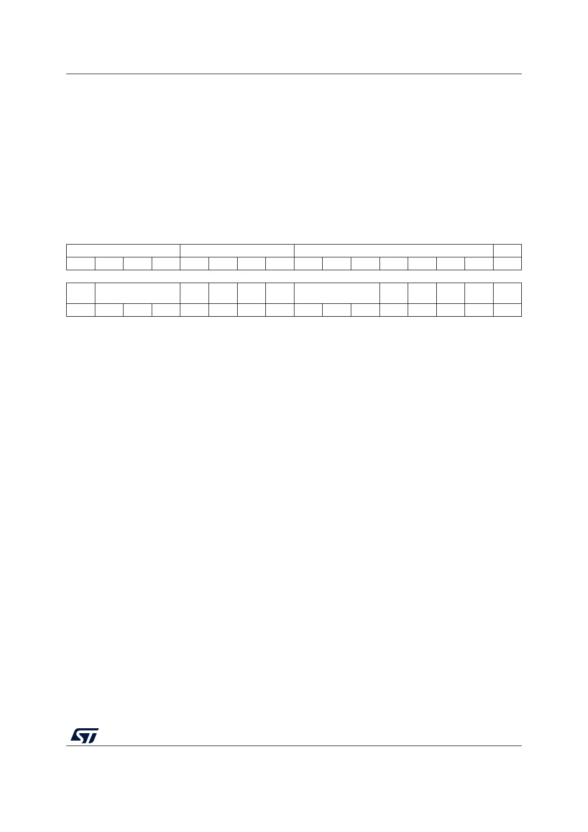
18.6.1 TSC control register (TSC_CR)
Address offset: 0x00
Reset value: 0x0000 0000
31 30 29 28 27 26 25 24 23 22 21 20 19 18 17 16
CTPH[3:0] CTPL[3:0] SSD[6:0] SSE
rw rw rw rw rw rw rw rw rw rw rw rw rw rw rw rw
1514131211109876543210
SSPSC PGPSC[2:0] Res. Res. Res. Res. MCV[2:0] IODEF
SYNC
POL
AM START TSCE
rw rw rw rw rw rw rw rw rw rw rw rw
Bits 31:28 CTPH[3:0]: Charge transfer pulse high
These bits are set and cleared by software. They define the duration of the high state of the
charge transfer pulse (charge of C
X
).
0000: 1x t
PGCLK
0001: 2x t
PGCLK
...
1111: 16x t
PGCLK
Note: These bits must not be modified when an acquisition is ongoing.
Bits 27:24 CTPL[3:0]: Charge transfer pulse low
These bits are set and cleared by software. They define the duration of the low state of the
charge transfer pulse (transfer of charge from C
X
to C
S
).
0000: 1x t
PGCLK
0001: 2x t
PGCLK
...
1111: 16x t
PGCLK
Note: These bits must not be modified when an acquisition is ongoing.
Note: Some configurations are forbidden. Refer to the Section 18.3.4: Charge transfer
acquisition sequence for details.
Bits 23:17 SSD[6:0]: Spread spectrum deviation
These bits are set and cleared by software. They define the spread spectrum deviation which
consists in adding a variable number of periods of the SSCLK clock to the charge transfer
pulse high state.
0000000: 1x t
SSCLK
0000001: 2x t
SSCLK
...
1111111: 128x t
SSCLK
Note: These bits must not be modified when an acquisition is ongoing.