AES hardware accelerator (AES) RM0367
452/1043 RM0367 Rev 7
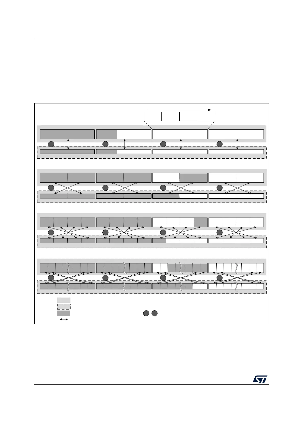
The data swap type is selected through the DATATYPE[1:0] bitfield of the AES_CR register.
The selection applies both to the input and the output of the AES core.
For different data swap types, Figure 100 shows the construction of AES processing core
input buffer data P127..0, from the input data entered through the AES_DINR register, or the
construction of the output data available through the AES_DOUTR register, from the AES
processing core output buffer data P127..0.
Figure 100. 128-bit block construction with respect to data swap
Note: The data in AES key registers (AES_KEYRx) and initialization registers (AES_IVRx) are not
sensitive to the swap mode selection.
MSv42153V2
DATATYPE[1:0] = 00: no swapping
Word 2Word 3
D127 D96
P95
LSBMSB
DATATYPE[1:0] = 01: 16-bit (half-word) swapping
Word 3
DATATYPE[1:0] = 10: 8-bit (byte) swapping
Word 2Word 3
DATATYPE[1:0] = 11: bit swapping
Word 3
LSB
MSB
LSB
MSB
LSBMSB
LSBMSB
MSB
MSB
MSB
LSB
LSB
Word 0Word 1
LSB
Word 0
Word 0Word 1
D63 D32
D31 D0
D64
Word 2
Zero padding (example)
Legend:
Data swap
Word 2
D95
Word 1
Word 0Word 1
AES input/output data block in memory
AES core input/output buffer data
1
1
1
1
2
2
2
2
3
3
3
3
4
4
4
4
Order of write to AES_DINR / read from AES_DOUTR
MSB
LSB
increasing memory address
D127 D96
D63 D32
D31 D0
D64D95
D127 D96 D95D112 D111 D80 D31 D0D15D16D64D79 D32D63 D48 D47
D127..120 D103..96D119..112 D111.104 D71...64D95..88 D87..80 D79..72 D63...56 D55...48 D47...40 D39...32 D31...24 D23...16 D15...8 D7...0
D127 D126 D125 D98 D97 D96 D95 D94 D93 D31 D30 D29 D0D1D2D66 D65 D64 D63 D62 D61 D34 D33 D32
byte 3 byte 2 byte 1 byte 0
D63 D55 D47 D39D56 D48 D40 D32
most significant bit (127) of memory data block / AEC core buffer
least significant bit (0) of memory data block / AEC core buffer
Dx input/output data bit ‘x’
D96D111 D127 D112 D64D79 D95 D80 D32D47 D63 D48 D0D15 D31 D16
D103..96 D111.104 D119..112 D127..120 D71...64 D79..72 D87..80 D95..88 D39...32 D47...40 D55...48 D63...56 D7...0 D15...8 D23...16 D31...24
D96 D127D97 D126D98 D125 D95D64 D94D65 D93D66 D63D32 D62D33 D61D34 D31D0 D30D1 D29D2
1 4