RM0367 Rev 7 71/1043
RM0367 Flash program memory and data EEPROM (FLASH)
122
3.3.2 Dual-bank boot capability
Category 5 devices have two Flash memory banks: Bank 1 and Bank 2. They feature an
additional boot mechanism which allows booting either from Bank 2 or from Bank 1
depending on BFB2 bit status (bit 23 in FLASH_OPTR register).
• When the BFB2 bit is set and the boot pins are configured to boot from Flash memory
(BOOT0 = 0 and BOOT1 = x), the device maps the System memory at address 0. It
boots from the System memory after reset and Standby and executes (during
approximately 440 µs)
the embedded bootloader code which implements the dual-
bank boot mechanism:
a) The System memory code first checks Bank 2. If it contains a valid code (see note
below), it sets the UFB bit in SYSCFG_CFGR1 register to map Bank 2 at address
0x0800 0000, jumps to the application code located in Bank 2, and leaves the
bootloader.
b) If the code located in Bank 2 is not valid, the System memory code checks Bank 1
code. If it is valid (see note below), it jumps to the application located in Bank 1
(UFB is kept at ‘0’ so that Bank 1 remains mapped at address 0x0800 0000).
c) If both Bank 2 and Bank 1 do not contain valid code (see note below), the normal
bootloader operations are executed when the protection level2 is disabled.
Otherwise, the System memory code jumps to Bank 1 regardless of its validity.
Refer to Table 11 for more details.
• When BFB2 bit is reset (default state), the dual-bank boot mechanism is not performed.
Note: The code is considered as valid when the first data located at the bank start address (which
should be the stack pointer) points to a valid address (stack top address).
For category 5 devices, the Flash memory Bank 1 and Bank 2, System memory or SRAM
can be selected as the boot area, as shown in Table 11 below.
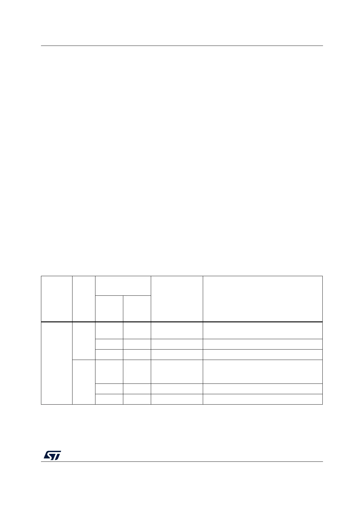
Table 11. Boot pin and BFB2 bit configuration
Protection
level
BFB2
bit
Boot mode
selection
Boot mode Aliasing
nBOOT1
option
bit
BOOT0
pin
0 or 1
0
X 0 User Flash memory
User Flash memory Bank1 is selected as the
boot area.
1 1 System memory Boot on System memory to execute bootloader.
0 1 Embedded SRAM Boot on Embedded SRAM
1
X 0 System memory
Boot on System memory to execute dual bank
boot mechanism. If Bank 2 and Bank 1are not
valid, bootloader is executed for Flash update.
1 1 System memory Boot on System memory to execute bootloader.
0 1 Embedded SRAM Boot on Embedded SRAM.