System configuration controller (SYSCFG) RM0367
256/1043 RM0367 Rev 7
10.2 SYSCFG registers
The peripheral registers have to be accessed by words (32-bit).
10.2.1 SYSCFG memory remap register (SYSCFG_CFGR1)
This register is used for specific configurations related to memory remap:
Note: This register is not reset through the SYSCFGRST bit in the RCC_APB2RSTR register.
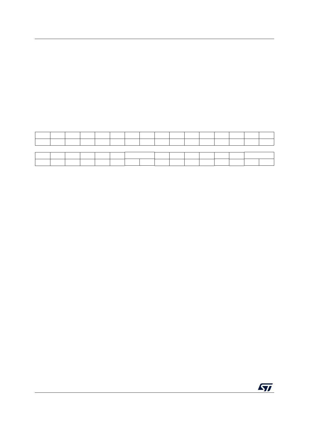
Address offset: 0x00
Reset value: 0x000x 000x (X is the memory mode selected by the boot configuration).
)
31 30 29 28 27 26 25 24 23 22 21 20 19 18 17 16
Res. Res. Res. Res. Res. Res. Res. Res. Res. Res. Res. Res. Res. Res. Res. Res.
1514131211109876543210
Res. Res. Res. Res. Res. Res. BOOT_MODE Res. Res. Res. Res. UFB Res. MEM_MODE
r r rw rw rw
Bits 31:10 Reserved, must be kept at reset value
Bits 9:8 BOOT_MODE: Boot mode selected by the boot pins status bits
These bits are read-only. They indicate the boot mode selected by the BOOT pins. Bit 9
corresponds to the complement of nBOOT1 bit in the FLASH_OPTR register. Its value is
defined in the option bytes. Bit 8 corresponds to the value sampled on BOOT0 pin (see
Section 2.4: Boot configuration on page 64).
00: Main Flash memory boot mode
01: System Flash memory boot mode
10: Reserved
11: Embedded SRAM boot mode
Bits 7:4 Reserved, must be kept at reset value