RM0367 Rev 7 315/1043
RM0367 Analog-to-digital converter (ADC)
352
the need for software having to set the ADSTART bit again and ensures the next trigger
event is not missed.
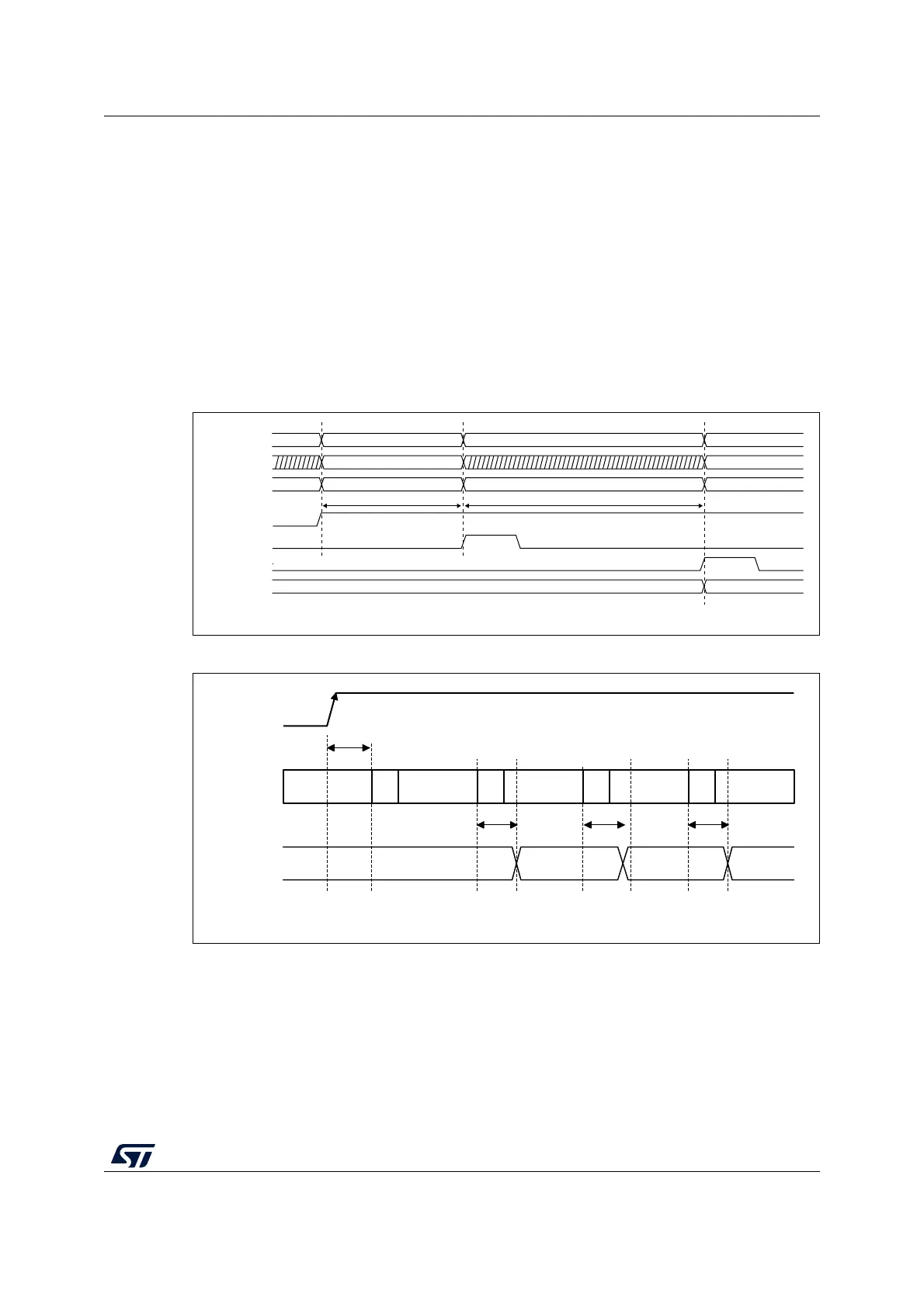
14.3.13 Timings
The elapsed time between the start of a conversion and the end of conversion is the sum of
the configured sampling time plus the successive approximation time depending on data
resolution:
Figure 37. Analog to digital conversion time
Figure 38. ADC conversion timings
1. EXTEN = 00 or EXTEN ≠ 00
2. Trigger latency (refer to datasheet for more details)
3. ADC_DR register write latency (refer to datasheet for more details)
t
CONV
= t
SMPL
+ t
SAR
= [ 1.5
|min
+ 12.5
|12bit
] x t
ADC_CLK
t
CONV
= t
SMPL
+ t
SAR
= 93.8 ns
|min
+ 781.3 ns
|12bit
= 0.875 µs
|min
(for f
ADC_CLK
= 16 MHz)
Analog
channel
Internal S/H
tt
depends on SMP[2:0]
set
by SW
EOSMP
cleared by SW
MS30336V1
DATA N-1
DATA N
CH(N)
CH(N+1)
ADC state
ADSTART
ADC_DR
EOC
SMPL
RDY
SAMPLING CH(N)
CONVERTING CH(N)
SAMPLING CH(N+1)
Sample AIN(N+1)
Hold AIN(N)
Sample AIN(N+1)
SAR
(1) (2)
set by HW
cleared
by SW
set
by HW
(1)
t
SMPL
depends on RES[2:0]
(2)
t
SAR
MSv33174V1
Ready S0 Conversion 0
t
LATENCY
(2)
ADSTART
(1)
ADC state
ADC_DR
S1 Conversion 1 S2 Conversion 2 S3 Conversion 3
W
LATENCY
(3)
W
LATENCY
(3)
W
LATENCY
(3)
Data 1Data 0 Data 2
 Loading...


